
INTRODUCTION
The embedded Write-Back Enhanced IntelDX4™ processor provides high performance to 32-bit, embedded applications. Designed for applications that need a floating-point unit, the processor is ideal for embedded designs running DOS*, Microsoft Windows*, OS/2*, or UNIX* applications written for the Intel architecture. Projects can be completed quickly using the wide range of software tools, utilities, assemblers and compilers that are available for desktop computer systems. Also, developers can find advantages in using existing chipsets and peripheral components in their embedded designs.
■ Up to 100 MHz Operation
■ Integrated Floating-Point Unit
■ Speed-Multiplying Technology
■ 32-Bit RISC Technology Core
■ 16-Kbyte Write-Back Cache
■ 3.3 V Core Operation with 5 V Tolerant I/O Buffers
■ Burst Bus Cycles
■ Dynamic Bus Sizing for 8- and 16-bit Data Bus Devices
■ SL Technology
■ Data Bus Parity Generation and Checking
■ Boundary Scan (JTAG)
■ 3.3-Volt Processor, 75 MHz, 25 MHz CLK
— 208-Lead Shrink Quad Flat Pack (SQFP)
■ 3.3-Volt Processor, 100 MHz, 33 MHz CLK
— 208-Lead Shrink Quad Flat Pack (SQFP)
— 168-Pin Pin Grid Array (PGA)
■ Binary Compatible with Large Software Base
The Intel 80486, also known as the i486 or 486, is a higher performance follow-up to the Intel 80386 microprocessor. The 80486 was introduced in 1989 and was the first tightly pipelined x86 design as well as the first x86 chip to use more than a million transistors, due to a large on-chip cache and an integrated floating-point unit. It represents a fourth generation of binary compatible CPUs since the original 8086 of 1978. A 50 MHz 80486 executes around 40 million instructions per second on average and is able to reach 50 MIPS peak performance. Approximately twice as fast as the 80386 or 80286 per clock cycle, thanks to its five stage pipeline with all stages bound to a single cycle. The on chip enhanced FPU unit was also significantly faster than the 80387 per cycle.
1. Background
The 80486 was announced at Spring Comdex in April 1989. At the announcement, Intel stated that samples would be available in the third quarter of 1989 and production quantities would ship in the fourth quarter of 1989.[1] The first 80486-based PCs were announced in late 1989, but some advised that people wait until 1990 to purchase an 80486 PC because there were early reports of bugs and software incompatibilities.[2]
2. Improvements
The 486DX2 architecture
The instruction set of the i486 is very similar to its predecessor, the Intel 80386, with the addition of only a few extra instructions, such as CMPXCHG which implements a compare-and-swap atomic operation and XADD, a fetch-and-add atomic operation returning the original value (unlike a standard ADD which returns flags only).
From a performance point of view, the architecture of the i486 is a vast improvement over the 80386. It has an on-chip unified instruction and data cache, an on-chip floating-point unit (FPU) and an enhanced bus interface unit. Due to the tight pipelining, sequences of simple instructions (such as ALU reg,reg and ALU reg,im) could sustain a single clock cycle throughput (one instruction completed every clock). These improvements yielded a rough doubling in integer ALU performance over the 386 at the same clock rate. A 16-MHz 80486 therefore had a performance similar to a 33-MHz 386, and the older design had to reach 50 MHz to be comparable with a 25-MHz 80486 part.[3]
2.1. Differences between i386 and i486
- An 8 KB on-chip (level 1) SRAM cache stores the most recently used instructions and data (16 KB and/or write-back on some later models). The 386 had no such internal cache but supported a slower off-chip cache (which was not a level 2 cache because there was no internal level 1 cache on the 80386).
- An enhanced external bus protocol to enable cache coherency and a new burst mode for memory accesses to fill a cacheline of 16 bytes within 5 bus cycles. The 386 needed 8 bus cycles to transfer the same amount of data.
- Tightly-coupled[4] pipelining completes a simple instruction like ALU reg,reg or ALU reg,im every clock cycle (after a latency of several cycles). The 386 needed two clock cycles to do this.
- Integrated FPU (disabled or absent in SX models) with a dedicated local bus; together with faster algorithms on more extensive hardware than in the i387, this performs floating point calculations faster compared to the i386+i387 combination.
- Improved MMU performance.
- New instructions: XADD, BSWAP, CMPXCHG, INVD, WBINVD, INVLPG.
Just as in the 80386, a simple flat 4 GB memory model could be implemented by setting all «segment selector» registers to a neutral value in protected mode, or setting (the same) «segment registers» to zero in real mode, and using only the 32-bit «offset registers» (x86-terminology for general CPU registers used as address registers) as a linear 32-bit virtual address bypassing the segmentation logic. Virtual addresses were then normally mapped onto physical addresses by the paging system except when it was disabled. (Real mode had no virtual addresses.) Just as with the 80386, circumventing memory segmentation could substantially improve performance in some operating systems and applications.
On a typical PC motherboard, either four matched 30-pin (8-bit) SIMMs or one 72-pin (32-bit) SIMM per bank were required to fit the 80486’s 32-bit data bus. The address bus used 30-bits (A31..A2) complemented by four byte-select pins (instead of A0,A1) to allow for any 8/16/32-bit selection. This meant that the limit of directly addressable physical memory was 4 gigabytes as well (230 32-bit words = 232 8-bit words).
3. Models
There are several suffixes and variants. (see Table). Other variants include:
- Intel RapidCAD: a specially packaged Intel 486DX and a dummy floating-point unit (FPU) designed as pin-compatible replacements for an Intel 80386 processor and 80387 FPU.
- i486SL-NM: i486SL based on i486SX.
- i487SX (P23N): i486DX with one extra pin sold as an FPU upgrade to i486SX systems; When the i487SX was installed, it ensured that an i486SX was present on the motherboard but disabled it, taking over all of its functions.
- i486 OverDrive (P23T/P24T): i486SX, i486SX2, i486DX2 or i486DX4. Marked as upgrade processors, some models had different pinouts or voltage-handling abilities from «standard» chips of the same speed stepping. Fitted to a coprocessor or «OverDrive» socket on the motherboard, worked the same as the i487SX.
The specified maximal internal clock frequency (on Intel’s versions) ranged from 16 to 100 MHz. The 16 MHz i486SX model was used by Dell Computers.
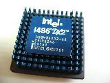
One of the few 80486 models specified for a 50 MHz bus (486DX-50) initially had overheating problems and was moved to the 0.8-micrometre fabrication process. However, problems continued when the 486DX-50 was installed in local-bus systems due to the high bus speed, making it rather unpopular with mainstream consumers, as local-bus video was considered a requirement at the time, though it remained popular with users of EISA systems. The 486DX-50 was soon eclipsed by the clock-doubled i486DX2, which although running the internal CPU logic at twice the external bus speed (50 MHz), was nevertheless slower due to the external bus running at only 25 MHz. The i486DX2 at 66 MHz (with 33 MHz external bus) was faster than the 486DX-50, overall.
More powerful 80486 iterations such as the OverDrive and DX4 were less popular (the latter available as an OEM part only), as they came out after Intel had released the next-generation P5 Pentium processor family. Certain steppings of the DX4 also officially supported 50 MHz bus operation, but it was a seldom used feature.
-
Model CPU/bus
clock speedVoltage L1 cache* Introduced Notes 
center|80px

i486DX (P4) 20, 25 MHz
33 MHz
50 MHz5 V 8 KB WT April 1989
May 1990
June 1991The original chip without clock multiplier 
i486SL 20, 25, 33 MHz 5 V or 3.3 V 8 KB WT November 1992 Low-power version of the i486DX, reduced VCore, SMM (System Management Mode), stop clock, and power-saving features — mainly for use in portable computers 
i486SX (P23) 16, 20, 25 MHz
33 MHz5 V 8 KB WT September 1991
September 1992An i486DX with the FPU part disabled or missing. Early variants were parts with disabled (defective) FPUs.[5] Later versions had the FPU removed from the die to reduce area and hence cost. 
i486DX2 (P24) 40/20, 50/25 MHz
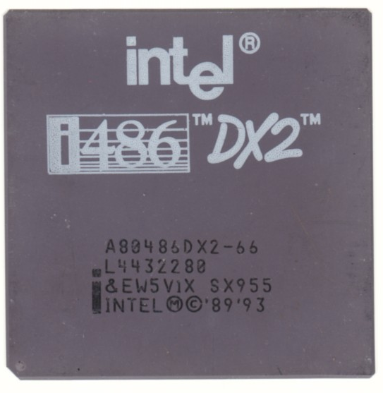
66/33 MHz5 V 8 KB WT March 1992
August 1992The internal processor clock runs at twice the clock rate of the external bus clock 
i486DX-S (P4S) 33 MHz; 50 MHz 5 V or 3.3 V 8 KB WT June 1993 SL Enhanced 486DX 
i486DX2-S (P24S) 40/20 MHz,
50/25 MHz,
(66/33 MHz)5 V or 3.3 V 8 KB WT June 1993 
i486SX-S (P23S) 25, 33 MHz 5 V or 3.3 V 8 KB WT June 1993 SL Enhanced 486SX 
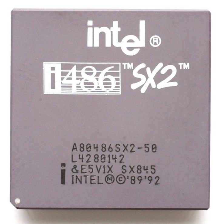
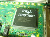
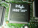
i486SX2 50/25, 66/33 MHz 5 V 8 KB WT March 1994 i486DX2 with the FPU disabled 
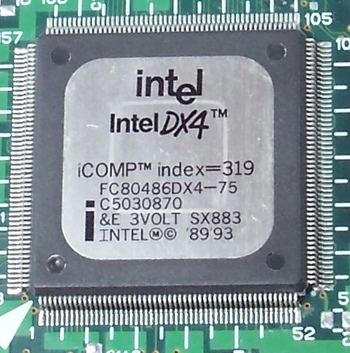
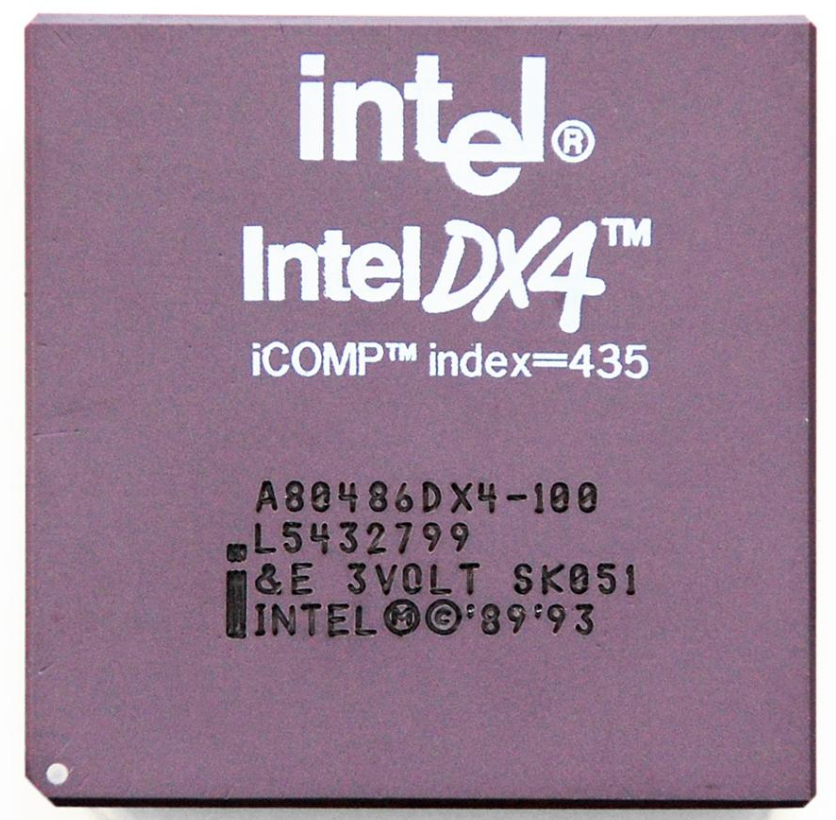
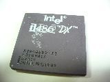
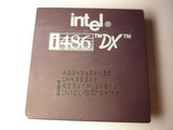
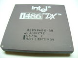
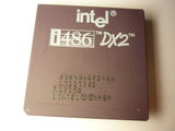
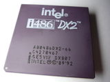
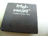
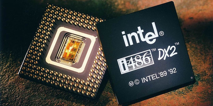
IntelDX4 (P24C) 75/25, 100/33 MHz 3.3 V 16 KB WT March 1994 Designed to run at triple clock rate (not quadruple, as often believed; the DX3, which was meant to run at 2.5× the clock speed, was never released). DX4 models that featured write-back cache were identified by an «&EW» laser-etched into their top surface, while the write-through models were identified by «&E». 
i486DX2WB (P24D) 50/25 MHz,
66/33 MHz5 V 8 KB WB October 1994 Enabled write-back cache. 
IntelDX4WB 100/33 MHz 3.3 V 16 KB WB October 1994 
i486DX2 (P24LM) 90/30 MHz,
100/33 MHz2.5–2.9 V 8 KB WT 1994 
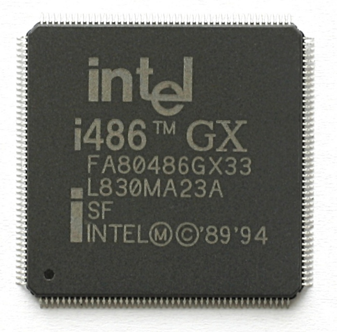
i486GX up to 33 MHz 3.3 V 8 KB WT Embedded ultra-low-power CPU with all features of the i486SX and 16-bit external data bus. This CPU is for embedded battery-operated and hand-held applications.
*WT = write-through cache strategy, WB = write-back cache strategy
4. Other Makers of 80486-Like CPUs
STMicroelectronics’ ST ST486DX2-40
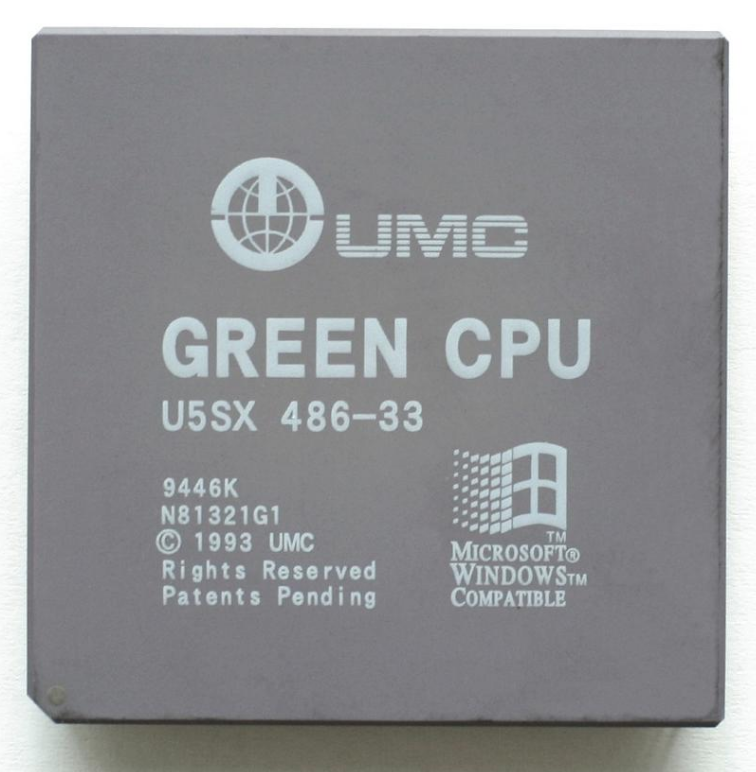
UMC Green CPU U5SX
80486 compatible processors have been produced by other companies such as IBM, Texas Instruments, AMD, Cyrix, UMC, and SGS Thomson. Some were clones (identical at the microarchitectural level), others were clean room implementations of the Intel instruction-set. (IBM’s multiple source requirement is one of the reasons behind its x86-manufacturing since the 80286.) The 80486 was, however, covered by many of Intel’s patents covering new R&D as well as that of the prior 80386. Intel and IBM have broad cross-licenses of these patents, and AMD was granted rights to the relevant patents in the 1995 settlement of a lawsuit between the companies.[6]
AMD produced several clones of the 80486 using a 40 MHz bus (486DX-40, 486DX/2-80, and 486DX/4-120) which had no equivalent available from Intel, as well as a part specified for 90 MHz, using a 30 MHz external clock, that was sold only to OEMs. The fastest running 80486 CPU, the Am5x86, ran at 133 MHz and was released by AMD in 1995. 150 MHz and 160 MHz parts were planned but never officially released.
Cyrix made a variety of 80486-compatible processors, positioned at the cost-sensitive desktop and low-power (laptop) markets. Unlike AMD’s 80486 clones, the Cyrix processors were the result of clean-room reverse-engineering. Cyrix’s early offerings included the 486DLC and 486SLC, two hybrid chips which plugged into 386DX or SX sockets respectively, and offered 1 KB of cache (versus 8 KB for the then-current Intel/AMD parts). Cyrix also made «real» 80486 processors, which plugged into the i486’s socket and offered 2 or 8 KB of cache. Clock-for-clock, the Cyrix-made chips were generally slower than their Intel/AMD equivalents, though later products with 8 KB caches were more competitive, if late to market.
The Motorola 68040, while not compatible with the 80486, was often positioned as the 80486’s equivalent in features and performance. Clock-for-clock basis the Motorola 68040 could significantly outperform the Intel 80486 chip.[7][8] However, the 80486 had the ability to be clocked significantly faster without suffering from overheating problems. The Motorola 68040 performance lagged behind the later production 80486 systems.
5. Motherboards and Buses
The first 80486 system from the UK on the cover of BYTE, September 1989
Early 80486 machines were equipped with several ISA slots (using an emulated PC/AT-bus) and sometimes one or two 8-bit–only slots (compatible with the PC/XT-bus).[9] Many motherboards enabled overclocking of these up from the default 6 or 8 MHz to perhaps 16.7 or 20 MHz (half the i486 bus clock) in a number of steps, often from within the BIOS setup. Especially older peripheral cards normally worked well at such speeds as they often used standard MSI chips instead of slower (at the time) custom VLSI designs. This could give significant performance gains (such as for old video cards moved from a 386 or 286 computer, for example). However, operation beyond 8 or 10 MHz could sometimes lead to stability problems, at least in systems equipped with SCSI or sound cards.
Some motherboards came equipped with a 32-bit bus called EISA that was backward compatible with the ISA-standard. EISA offered a number of attractive features such as increased bandwidth, extended addressing, IRQ sharing, and card configuration through software (rather than through jumpers, DIP switches, etc.) However, EISA cards were expensive and therefore mostly employed in servers and workstations. Consumer desktops often used the simpler but faster VESA Local Bus (VLB), unfortunately somewhat prone to electrical and timing-based instability; typical consumer desktops had ISA slots combined with a single VLB slot for a video card. VLB was gradually replaced by PCI during the final years of the 80486 period. Few Pentium class motherboards had VLB support as VLB was based directly on the i486 bus; it was no trivial matter adapting it to the quite different P5 Pentium-bus. ISA persisted through the P5 Pentium generation and was not completely displaced by PCI until the Pentium III era.
Late 80486 boards were normally equipped with both PCI and ISA slots, and sometimes a single VLB slot as well. In this configuration VLB or PCI throughput suffered depending on how buses were bridged. Initially, the VLB slot in these systems was usually fully compatible only with video cards (quite fitting as «VESA» stands for Video Electronics Standards Association); VLB-IDE, multi I/O, or SCSI cards could have problems on motherboards with PCI slots. The VL-Bus operated at the same clock speed as the i486-bus (basically being a local 80486-bus) while the PCI bus also usually depended on the i486 clock but sometimes had a divider setting available via the BIOS. This could be set to 1/1 or 1/2, sometimes even 2/3 (for 50 MHz CPU clocks). Some motherboards limited the PCI clock to the specified maximum of 33 MHz and certain network cards depended on this frequency for correct bit-rates. The ISA clock was typically generated by a divider of the CPU/VLB/PCI clock (as implied above).
One of the earliest complete systems to use the 80486 chip was the Apricot VX FT, produced by British hardware manufacturer Apricot Computers. Even overseas in the United States it was popularised as «The World’s First 80486» in the September 1989 issue of Byte magazine (shown right).
Later 80486 boards also supported Plug-And-Play, a specification designed by Microsoft that began as a part of Windows 95 to make component installation easier for consumers.
6. Gaming
The 486DX2 66 MHz processor was popular on home-oriented PCs during the early to mid 1990s, toward the end of the MS-DOS gaming era. It was often coupled with a VESA Local Bus video card.
The introduction of 3D computer graphics spelled the end of the 80486’s reign, because 3D graphics make heavy use of floating-point calculations and require a faster CPU cache and more memory bandwidth. Developers began to target the P5 Pentium processor family almost exclusively with x86 assembly language optimizations (e.g., Quake) which led to the usage of terms like «Pentium-compatible processor» for software requirements. Many of these games required the speed of the P5 Pentium processor family’s double-pipelined architecture.
7. Obsolescence
The AMD Am5x86, up to 133 MHz, and Cyrix Cx5x86, up to 120 MHz, were the last 80486 processors that were often used in late generation 80486 motherboards with PCI slots and 72-pin SIMMs that are designed to be able to run Windows 95, and also often used as upgrades for older 80486 motherboards. While the Cyrix Cx5x86 faded quite quickly when the Cyrix 6×86 took over, the AMD Am5x86 was important during the time when the AMD K5 was delayed.
80486-based machines remained popular through the late 1990s, serving as low end processors for entry level PCs. Production for traditional desktop and laptop systems ceased in 1998, when Intel introduced the Celeron brand as an modern replacement for the aging chip, though it continued to be produced for embedded systems through the late 2000s.
In the general-purpose desktop computer role, 80486-based machines remained in use into the early 2000s, especially as Windows 95, Windows 98, and Windows NT 4.0 were the latest Microsoft operating systems to officially support installation on an 80486-based system.[10][11] However, as Windows 95/98 and Windows NT 4.0 were eventually overtaken by newer operating systems, 80486 systems likewise fell out of use. Still, a number of 80486 machines have remained in use today, mostly for backward compatibility with older programs (most notably games), especially since many of them have problems running on newer operating systems. However, DOSBox is also available for current operating systems and provides emulation of the 80486 instruction set, as well as full compatibility with most DOS-based programs.[12]
Although the 80486 was eventually overtaken by the Pentium for personal computer applications, Intel had continued production for use in embedded systems. In May 2006 Intel announced that production of the 80486 would stop at the end of September 2007.[13]
КомпьютерПресс №3 1993. А. Борзенко

Интегральная схема микропроцессора i80486 была анонсирована фирмой Intel в
1989 году на выставке Comdex в Чикаго. И хотя, очевидно, нам не долго уже
осталось ждать появления нового 586-го микропроцессора, на сегодняшний
день одним из самых мощных универсальных микропроцессоров является i80486.
Архитектура микропроцессора i80486
«В архитектуре взаимосвязаны функциональные, технические и эстетические
начала — польза, прочность, красота».
(Из словаря)
Микропроцессор i80486 достойный продолжатель семейства i80x86‚ поскольку
он позволяет создавать вычислительные системы намного более
производительные, чем, предположим, на микропроцессоре i80386. В принципе
микросхема i80486 состоит из полного микропроцессора i80386,
арифметического сопроцессора i80387 и контроллера кэш-памяти i82385.
Понятно, что речь не идет о механическом соединении функциональных
устройств на одном кристалле. Высокая степень интеграции (более миллиона
транзисторов) — это не просто технологическое достижение, а возможность
реализовать новые архитектурные решения, которые позволяют повысить
производительность микропроцессора. Так, например, в микропроцессоре
i80486 используется конвейерная обработка команд, достаточно широко
применяемая в RISC-процессорах. При одной и той же тактовой частоте с
i80386 микропроцессор i80486 работает в три-четыре раза производительнее.
Это связано с уменьшением количества циклов (тактов), необходимых для
выполнения команды (инструкции).
Три в одном
На рис. 1 приведена примерная блок-схема микропроцессора i80486, на
которой достаточно легко выделить его основные функциональные узлы —
устройство управления памятью (Memory Management Unit, MMU), модуль
арифметического сопроцессора (Floating Point Unit, FPU) и блок кэш-памяти
(Cache Unit). Несмотря на то, что микропроцессор i80486 обладает всеми
свойствами, присущими i80386, имеются, конечно, и различия. Например, в
набор команд микропроцессора i80486 наряду с известными инструкциями для
i80386, включено несколько дополнительных команд. Однако устройство
управления памятью MMU полностью совместимо с аналогичным устройством в
i80386. То же можно сказать и о FPU. А это, вообще говоря, означает, что
все программное обеспечение, работающее на серии микропроцессоров
80×86/80×87, без внесения каких-либо изменений будет работать и на i80486.

Устройство управления памятью MMU состоит в свою очередь из устройства
сегментации (Segmentation Unit) и устройства управления страницами (Paging
Unit). Благодаря делению памяти на сегменты (сегментации) коды программ и
области данных могут находиться практически в любом месте логического
адресного пространства. Иными словами, при сегментной организации памяти
каждый модуль занимает свою собственную сплошную область памяти, тогда как
при страничной организации модуль разбивается на отдельные страницы. В
свою очередь, устройство управления страницами позволяет реализовать
механизм страничной организации памяти, который функционирует на более
низком уровне и является прозрачным по отношению к процессу сегментации.
Это дает возможность управления физическим адресным пространством. Следует
также отметить, что страничная организация памяти (paging) может быть
отключена чисто программным способом.
Каждый сегмент памяти может подразделяться на один или несколько 4-Кбайтных блоков. А память, в свою очередь, может
быть организована в виде одного или нескольких таких сегментов, размер
которых может достигать 4 Гбайт. Причем каждому такому сегменту могут
придаваться соответствующие атрибуты, которые определяют его расположение
в памяти, величину, вид (стек, код, данные) и характеристику защиты.
Каждая задача, выполняемая на i80486, может в принципе состоять из 16
381 сегмента, по 4 Гбайта каждый. Таким образом, диапазон виртуальной
адресации достигает 64 Тбайт. Устройство сегментации микропроцессора
поддерживает четыре механизма защиты приложений и системного режима друг
от друга. Благодаря этому на базе микропроцессора i80486 возможно
построение высокозащищенных систем.
Принципиально микропроцессор i80486 имеет два режима работы: реальный
режим (Real Mode, иначе 8086-Mode) и защищенный (Protected Mode). При этом
в реальном режиме он ведет себя просто как очень быстрый микропроцессор
i8086. Из этого режима i80486 может легко переключиться в защищенный
режим, в котором имеются богатые возможности управления памятью. Например,
в этом режиме возможно переключение с одной задачи на другую, причем их
обработка будет происходить как обработка независимых задач на своих i8086
микропроцессорах (режим «виртуальных 8086-машин»). Такое название связано
с тем, что каждая задача ведет себя таким же образом, как если бы она
выполнялась на собственном процессоре i8086 (соответственно i8088).
Устройство арифметического сопроцессора в i80486 работает параллельно с
АЛУ и поддерживает большое количество арифметических команд для различных
типов операндов. Это, в частности, многочисленные трансцендентные функции,
такие как синус, косинус, тангенс, логарифм и т.д. Нужно отметить, что FPU
полностью поддерживает стандарт ANSI/IEEE 754-1985
на арифметические операции с плавающей точкой.
Размер внутренней кэш-памяти микропроцессора i80486 составляет 8
Кбайт. Сразу следует сказать, что для некоторых приложений такой размер
кэш-памяти вовсе не достаточен. Это касается в первую очередь САПР и
настольных издательских систем. Однако в этом случае при разработке
соответствующей системы можно воспользоваться кэш-контроллером i82485 и
внешней кэш-памятью объемом 64 или 128 Кбайт. Внутренняя кэш-память
выполнена как ассоциативная и работает в режиме write through (то есть
данные заносятся одновременно и в кэш-память, и в ОЗУ). Кэш в
микропроцессоре i80486, безусловно, имеет и некоторые особенности. В
частности, страницы памяти могут быть обозначены либо как «кэшируемые»,
либо как «некэшируемые», причем такое обозначение можно вводить как
аппаратно, так и программно. Впрочем, даже само устройство кэша может быть
также отключено как аппаратно, так и программно. По некоторым оценкам,
использование встроенной кэш-памяти экономит до 80% времени, необходимого
для обращения к ОЗУ.
Регистры, регистры, регистры…
Микропроцессор i80486 содержит, конечно, все регистры, имеющиеся в
микросхемах i80386 и i80387. Регистры рассматриваемого микропроцессора
можно условно подразделить на три большие группы: базовые регистры,
регистры системного уровня и регистры плавающей точки. Рассмотрим эти
группы регистров несколько подробнее.
Программная модель i80486 определяется главным образом базовыми
регистрами, которые приведены на рис. 2. Это — восемь 32-разрядных
регистров общего назначения, которые могут работать с операндами данных
размерами 1, 2 и 4 байта или полями бит от 1 до 32. Однако операнды адреса
могут иметь длину только либо 2, либо 4 байта. Эти
32-разрядные регистры обозначаются как EAX, EBX, ECX, EDX, ESI,
EDI, EBP и ESP. Обозначения двух младших байт этих регистров пользователям
микропроцессоров i8088/86/286 уже хорошо известны. Конечно, это — AX, BX,
CX, DX, SI, DI, BP и SP. Причем следует отметить, что при доступе к
старшим двум байтам этих 32-разрядных регистров содержимое двух младших
байтов не изменяется. Этим обуславливается совместимость сверху-вниз с
микропроцессором i80286. Операции с байтовыми операндами (старший и
младший байты) доступны только для четырех регистров AX, BX, CX, DX,
причем старшие байты соответствуют обозначениям AH, BH, CH и DH, а младшие
— AL, BL, CL и DL.


Регистр указателя команд (Instruction Pointer, EIP) — также 32-разрядный и указывает на следующую выполняемую команду,
конечно же, косвенно. Этот регистр указывает только смещение относительно
начала кодового сегмента адреса, который образуется с использованием
содержимого регистра CS и элемента дескрипторной таблицы (подробнее об
этом несколько позже). Два младших байта регистра EIP соответствую 16-разрядному регистру IP, который используется только
при 16-битной адресации.
Для обозначения базового 32—разрядного регистра
побитной индикации состояния процессора используется так называемый
регистр флагов — EFLAGS. Этот регистр содержит биты, характеризующие
последнюю выполненную процессором операцию, и некоторую другую служебную
информацию. На рис. 3 приведены обозначения битов в регистре EFLAGS.
Поясним назначение некоторых из них. Если в регистре EFLAGS установлен
17-й бит — VM (Virtual 8086 Mode), то
микропроцессор i80486 переходит в режим «виртуальных 8086-машин». Конечно,
это возможно только в защищенном режиме. Бит 16 — RF (Resume Flag)
используется обычно для отладочных режимов. При его установке прерывание,
вызванное фатальной ошибкой, игнорируется и выполняется переход на
следующую инструкцию. Бит 14 — NT (Nested Task) используется в i80486 для
наблюдения за несколькими прерванными или вызванными по инструкции CALL
программами. Два бита 12 и 13 IOPL (Input/Output Privilege Level)
определяют право доступа в защищенном режиме к инструкциям ввода-вывода.

Из шести 16-разрядных сегментных регистров
четыре (DS, ES, FS и GS) называются регистрами сегментов данных, CS —
регистром кодового сегмента, а SS — регистром сегмента стека. Как работают
эти регистры в режиме микропроцессора i8086, достаточно хорошо известно.
Для получения 20-разрядного физического адреса
необходимо суммировать 16-битное смещение с
базовым адресом, хранящимся в одном из сегментных регистров. Причем
сложение происходит так, что содержимое сегментного регистра сдвинуто
относительно второго слагаемого (смещения) влево на 4 разряда. То есть, по
сути, происходит сложение 20-битового базового
адреса (4 младших разряда которого, безусловно, всегда нули) с 16-битовым смещением, в результате, конечно, получается
необходимый 20-разрядный адрес. При работе же
микропроцессора i80486 (ну и, разумеется, i80386) в защищенном режиме
исполнительный физический адрес образуется несколько иначе. Можно сказать,
что он образуется из пяти компонент. Прежде всего отметим, что в
защищенном режиме сегментные регистры называются селекторными, или просто
селекторами. Селекторный регистр указывает на соответствующий элемент в
одной из Дескрипторных Таблиц, расположенных в памяти. Причем базовый
адрес этой Таблицы хранится либо в регистре Глобальной Дескрипторной
Таблицы, либо в регистре Локальной Дескрипторной Таблицы, хотя в общем
случае может храниться и в ином регистре микропроцессора. Каждый элемент
Дескрипторной Таблицы содержит базовый адрес определенного сегмента, его
величину и права
доступа. У i80486 элемент Глобальной Дескрипторной Таблицы имеет размер 8
байт и состоит из 32-разрядного базового адреса,
20-разрядного поля размера сегмента и атрибутов дескриптора. В поле
размера сегмента, например, может храниться либо количество байт (до 1
Мбайта), которое содержит данный сегмент, либо количество страниц по
4096 байт каждая. Следовательно, размер сегмента в защищенном режиме
может варьироваться от 1 байта до 4 Гбайт. Таким образом,
результирующий адрес в защищенном режиме может быть образован в общем
случае суммированием содержимого базового регистра с содержимым индексного
регистра, умноженного на масштабный коэффициент (1, 2, 4 или 8), плюс
смещение в самой команде и плюс базовый адрес сегмента из элемента
Дескрипторной Таблицы (рис. 4).

Микропроцессор i80486 имеет три управляющих регистра (Control Registers)
системного уровня — CR0, CR2, и CR3 (регистр CR1 зарезервирован фирмой
Intel для дальнейшего расширения). В регистре CR0 из имеющихся 32 бит
для целей управления и определения статуса используется только 10 (рис.
5). Причем 5 из этих 10 бит появились только в i80486 (в i80386
их нет). Это биты — CD, NW, AM, WP и NE. Функционально все эти 10 бит
характеризуют следующее: режимы микропроцессора i80486 — PG, PE, режимы
встроенного устройства кэш-памяти — CD, NW, встроенное устройство
управления плавающей арифметикой — TS, EM, MP и NE, управление контролем
выравнивания — AM, защита записи супервизора — WP. Младшее слово регистра
CR0 используется также в качестве статусного слова (слова состояния)
микропроцессора (Machine Status Word, MSW), для того чтобы сохранить
совместимость с защищенным режимом i80286. Следовательно, команды LMSW и
SMSW (Load MSW, Store MSW) действуют только для нижних 16 бит CR0 и
игнорируют новые биты. Для того чтобы можно было работать с этими новыми
битым, в набор команд микропроцессора i80486 включена специальная
инструкция MOV CR0, Reg.

В управляющем регистре CR2 накопится адрес, по которому появилась ошибка
при разбиении памяти на страницы. Управляющий регистр CR3 используется
только тогда, когда в регистре CR0 установлен бит PG. В этом случае
регистр содержит базовый адрес таблицы страниц, которые может использовать
микропроцессор для каждой задачи. Сама же эта таблица всегда выровнена на
одну страницу (4 Кбайт).
Четыре адресных системных регистра в микропроцессорах i80386/486
используются для таблиц или сегментов, которые хранятся в основной памяти.
Это — Глобальная Дескрипторная Таблица (Global Descriptor Table, GDT),
Локальная Дескрипторная Таблица (Local Descriptor Table, LDT),
Дескрипторная Таблица Прерываний (Interrupt Descriptor Table, IDT) и
Сегмент Состояния Задачи (Task State Segment, TSS). Для обозначений
соответствующих регистров используются аббревиатуры — GDTR, LDTR, IDTR и
TR. Регистры GDTR и IDTR содержат 32-разрядный
базовый адрес, а также 16-разрядную границу для
таблиц GDT и IDT. Таблицы GDT и IDT находятся в распоряжении всех задач
как глобальные сегменты, в то время как LDT и TSS зависят от конкретной
задачи. В регистрах LDTR и TR хранятся 16-разрядные
селекторы для выбора LDT и соответственно TSS-дескриптора.
Набор регистров для операций с плавающей точкой включает в себя восемь
80-разрядных регистров данных, 48-разрядные указатели данных и команд, а также
16-разрядные регистры управления, состояния и слова признаков.
Поскольку принцип работы FPU полностью соответствует работе i80387, а
арифметические сопроцессоры — хорошая тема для отдельного разговора,
подробно останавливаться на эти регистрах мы пока не будем.
В следующих выпусках нашего журнала мы обязательно вернемся к разговору о микропроцессорах фирмы Intel, и не только о них.
А. Борзенко
КомпьютерПресс 3’92
См. также описание семейства процессоров x86.
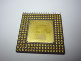
Intel 80486
![]()
486 SX
 A80486SX-25
A80486SX-25 E5V1X
KU80486SX-25 SX683
KU80486SX-25 SX800
KU80486SX-33
A80486SX-33
SB80486SX-33
486 SX2
A80486SX2-50
486 DX
A80486DX-33 SX419
A80486DX-33 SX810
A80486DX-50
486 DX2
SB80486DX2-40
SB80486DX2-50
A80486DX2-50 SX641
A80486DX2-50 SX808
A80486DX2-66 SX750
A80486DX2-66 Blue Heatsink SX759
A80486DX2-66 SX807
A80486DX2-66 (i66 marked) SX911
A80486DX2-66 SX955
486DX2-66 03H4-939-PQ (Mfg by IBM)
486 DX4
A80486DX4-75
FC80486DX4-75
A80486DX4-100 SK051
A80486DX4-100 SK096

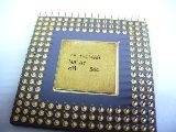
486 SX
| A80486SX-25 | ||
|
|
|
Frequency: 25 MHz Bus: 25 MHz Codename: P23 L1 Cache: 8 KB L2 Cache: — ID: SX679 Package: CPGA-168 Socket: Socket 1 Technology: 1 mcm Year: 1991 Top |
| A80486SX-25 &E5V1X | ||
|
|
|
Frequency: 25 MHz Bus: 25 MHz Codename: P23 L1 Cache: 8 KB L2 Cache: — ID: SX798 Package: CPGA-168 Socket: Socket 1 Technology: 1 mcm Year: 1994 Top |
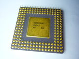
| KU80486SX-25 SX683 | ||
|
|
|
Frequency: 25 MHz Bus: 25 MHz Codename: P23 L1 Cache: 8 KB L2 Cache: — Writeback cache: No SL Enhanced: No ID: SX683 Package: PQFP-196 Socket: — Technology: 1 mcm Year: 1991 Top |
| KU80486SX-25 | ||
|
|
|
Frequency: 25 MHz Bus: 25 MHz Codename: P23 L1 Cache: 8 KB L2 Cache: — Writeback cache: No SL Enhanced: Yes ID: SX800 Package: PQFP-196 Socket: — Technology: 1 mcm Year: 1991 Top |
| KU80486SX-33 | ||
|
|
|
Frequency: 33 MHz Bus: 33 MHz Codename: P23 L1 Cache: 8 KB L2 Cache: — ID: SX849 Package: PQFP-196 Socket: — Technology: 1 mcm Year: 1994 Top |
| A80486SX-33 | ||
|
|
|
Frequency: 33 MHz Bus: 33 MHz Codename: P23 L1 Cache: 8 KB L2 Cache: — ID: SX797 Package: CPGA-168 Socket: Socket 1 Technology: 1 mcm Year: 1992 Top |
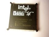
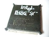
| SB80486SX-33 Mobile CPU with SL Enhanced technology |
||
|
|
|
Frequency: 33 MHz Bus: 33 MHz Codename: P23 L1 Cache: 8 KB L2 Cache: — ID: SX774 Package: PQFP-208 Socket: — Technology: 1 mcm Year: 1993 Top |

486 SX2
| A80486SX2-50 | ||
|
|
|
Frequency: 50 MHz Bus: 25 MHz Codename: P23 L1 Cache: 8 KB L2 Cache: External ID: SX845 Package: CPGA-168 Socket: Socket 1/2/3 Technology: 1 mcm Year: 1994 Top |
486 DX
| A80486DX-33 | ||
|
|
|
Frequency: 33 MHz Bus: 33 MHz Codename: P4 L1 Cache: 8 KB L2 Cache: — ID: SX419 Package: CPGA-168 Socket: Socket 1/2/3 Technology: 0.8 mcm Year: 1992 Top |
| A80486DX-33 SX810 SL enhanced version |
||
|
|
|
Frequency: 33 MHz Bus: 33 MHz Codename: P4 L1 Cache: 8 KB L2 Cache: — ID: SX810 Package: CPGA-168 Socket: Socket 1/2/3 Technology: 0.8 mcm Year: 1994 Top |
| A80486DX-50 | ||
|
|
|
Frequency: 50 MHz Bus: 50 MHz Codename: P4 L1 Cache: 8 KB L2 Cache: — ID: SX710 Package: CPGA-168 Socket: Socket 1/2/3 Technology: 0.8 mcm Year: 1993 Top |
486 DX2
| SB80486DX2-40 Mobile CPU with SL Enhanced technology |
||
|
|
|
Frequency: 40 MHz Bus: 20 MHz Codename: P24 L1 Cache: 8 KB L2 Cache: External ID: SX809 Package: PQFP-208 Socket: — Technology: 0.6 mcm Year: 1993 Top |
| SB80486DX2-50 Mobile CPU with SL Enhanced technology |
||
|
|
|
Frequency: 50 MHz Bus: 25 MHz Codename: P24 L1 Cache: 8 KB L2 Cache: External ID: SX825 Package: PQFP-208 Socket: — Technology: 0.6 mcm Year: 1994 Top |
| A80486DX2-50 SX641 | ||
|
|
|
Frequency: 50 MHz Bus: 25 MHz Codename: P24 L1 Cache: 8 KB L2 Cache: External Writeback cache: No SL Enhanced: No ID: SX641 Package: CPGA-168 Socket: Socket 1/2/3 Technology: 0.8 mcm Year: 1992 Top |
| A80486DX2-50 | ||
|
|
|
Frequency: 50 MHz Bus: 25 MHz Codename: P24 L1 Cache: 8 KB L2 Cache: External Writeback cache: No SL Enhanced: Yes ID: SX808 Package: CPGA-168 Socket: Socket 1/2/3 Technology: 0.8 mcm Year: 1992 Top |
| A80486DX2-66 SX750 | ||
|
|
|
Frequency: 66 MHz Bus: 33 MHz Codename: P24 L1 Cache: 8 KB L2 Cache: External ID: SX750 Package: CPGA-168 Socket: Socket 1/2/3 Technology: 0.8 mcm Year: 1992 Top |
| A80486DX2-66 Blue Heatsink SX759 | ||
|
|
|
Frequency: 66 MHz Bus: 33 MHz Codename: P24 L1 Cache: 8 KB L2 Cache: External ID: SX759 Package: CPGA-168 Socket: Socket 1/2/3 Technology: 0.8 mcm Year: 1992 Top |
| A80486DX2-66 SX807 | ||
|
|
|
Frequency: 66 MHz Bus: 33 MHz Codename: P24 L1 Cache: 8 KB L2 Cache: External ID: SX807 Package: CPGA-168 Socket: Socket 1/2/3 Technology: 0.8 mcm Year: 1992 Top |
| A80486DX2-66 (i66 marked) SX911 My first CPU in collection |
||
|
|
|
Frequency: 66 MHz Bus: 33 MHz Codename: P24 L1 Cache: 8 KB L2 Cache: External ID: SX911 Package: CPGA-168 Socket: Socket 1/2/3 Technology: 0.8 mcm Year: 1992 Top |
| 486DX2-66 03H4-939-PQ (Mfg by IBM) | ||
|
|
|
Frequency: 66 MHz Bus: 33 MHz Codename: P24 L1 Cache: 8 KB L2 Cache: External ID: — Package: CPGA-168 Socket: Socket 1/2/3 Technology: 0.8 mcm Year: 1993 Top |
| A80486DX2-66 A80486DX2-66 w/ Writeback cache |
||
|
|
|
Frequency: 66 MHz Bus: 33 MHz Codename: P24 L1 Cache: 8 KB L2 Cache: External ID: SX955 Package: CPGA-168 Socket: Socket 1/2/3 Technology: 0.8 mcm Year: 1995 Top |


486 DX4
| A80486DX4-75 SK047 | ||
|
|
|
Frequency: 75 MHz Bus: 25 MHz Codename: P24C L1 Cache: 8 KB L2 Cache: External ID: SK047 Package: CPGA-168 Socket: Socket 1/2/3 Technology: 0.6 mcm Year: 1995 Top |
| FC80486DX4-75 Mobile | ||
|
|
|
Frequency: 75 MHz Bus: 25 MHz Codename: P24C L1 Cache: 8 KB L2 Cache: External ID: SX883 Package: CPGA-168 Socket: Socket 1/2/3 Technology: 0.6 mcm Year: 1994 Top |
| A80486DX4-100 | ||
|
|
|
Frequency: 100 MHz Bus: 33 MHz Codename: P24C L1 Cache: 8 KB L2 Cache: External Writeback cache: No SL Enhanced: Yes ID: SK051 Package: CPGA-168 Socket: Socket 1/2/3 Technology: 0.6 mcm Year: 1994 Top |
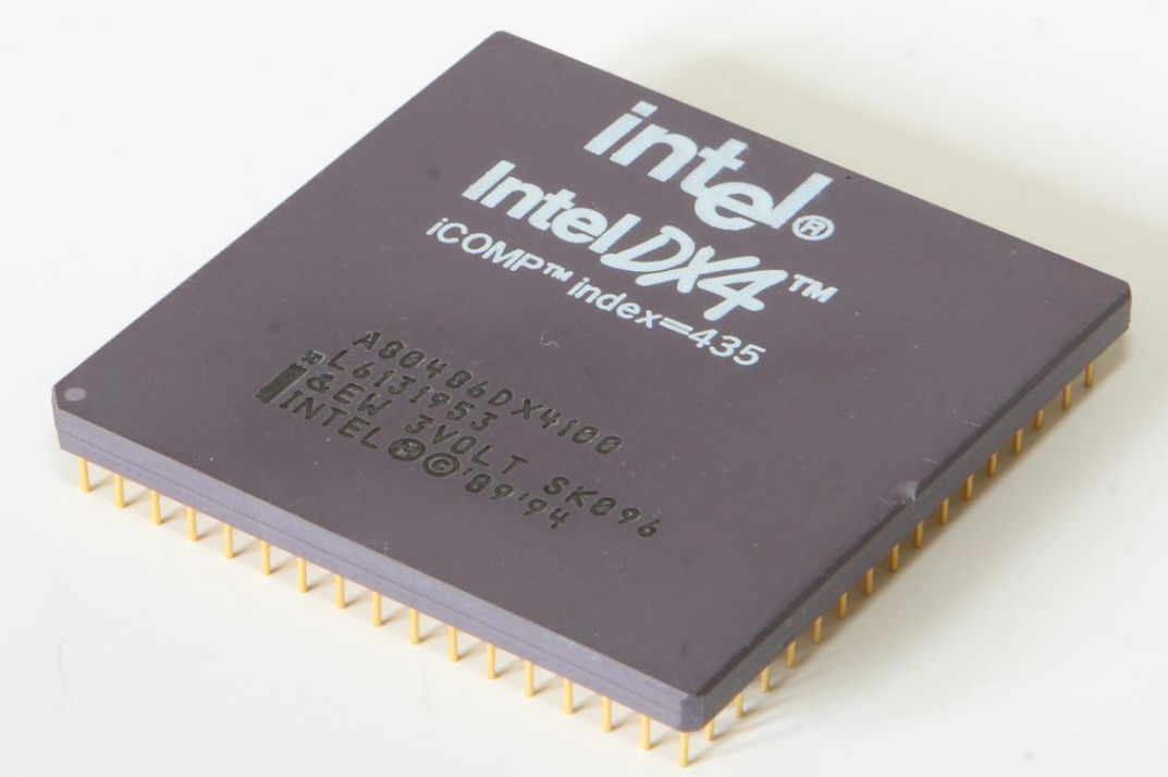
| A80486DX4100 SK096 A80486DX4100 w/ Writeback cache
|
||
|
|
|
Frequency: 100 MHz Bus: 33 MHz Codename: P24C L1 Cache: 8 KB L2 Cache: External Writeback cache: Yes SL Enhanced: Yes ID: SK096 Package: CPGA-168 Socket: Socket 1/2/3 Technology: 0.6 mcm Year: 1995 Top |

The Intel 80486 is a higher performance follow-up to the Intel 80386 microprocessor. Introduced in 1989, it is the first tightly pipelined x86
design as well as the first x86 chip to use more than a million transistors, due to a large on-chip cache and an integrated floating-point unit. It
represents a fourth generation of binary compatible CPUs since the original 8086 of 1978.
A 50 MHz 80486 executes around 40 million instructions per second on average and is able to reach 50 MIPS peak performance.
The i486 does not have the usual 80-prefix because of a court ruling that prohibits trademarking numbers (such as 80486). Later, with the introduction of the Pentium brand, Intel began branding its chips with words rather than numbers.
Switch to the die picture page!

|
A80486DX-25 Specification Details |
Show | |
|
A80486DX-33 Specification Details |
Show | |
|
A80486DX-50 Specification Details |
Show | |
An i486DX with the FPU part disabled or missing. Early variants were parts with disabled (defective) FPUs. Later versions had the FPU removed from the die to reduce area and hence cost.
|
A80486SX-16 Specification Details |
Show | |

|
A80486SX-25 Specification Details |
Show | |
|
A80486SX-33 Specification Details |
Show | |
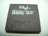
The internal processor clock runs at twice the clock rate of the external bus clock.
|
A80486DX2-50 Specification Details |
Show | |

|
A80486DX2-66 Specification Details |
Show | |
|
486DX2-66 03H4939 Specification Details |
Show | |
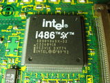
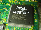
The i486 SX2 is an i486 SX with doubled internal frequency.

|
A80486SX2-50 Specification Details |
Show | |
Designed to run at triple clock rate (not quadruple as often believed; the DX3, which was meant to run at 2.5x the clock speed, was never released). DX4 models that featured write-back cache were
identified by an «&EW» laser etched into their top surface, while the write-through models were identified by «&E».
|
A80486DX4-75 Specification Details |
Show | |
|
A80486DX4-100 Specification Details |
Show | |
Unlisted models:
- i486 SX: 20 MHz
- i486 DX2: 40 MHz
- i486 SX2: 66 MHz
- i487 SX
Sumbit a picture or contribute to the museum!
RETURN TO INTEL

RETURN TO THE MAIN MUSEUM PAGE

PC Game Programmer’s guide was produced by me, Zack Smith.
HTML modifications are therefore copyrighted
© 2005, 2009 by Zack Smith all rights reserved.
This information is provided in the hope that it will be useful,
but without any warranty. It is provided AS-IS,
without even the implied warranty of fitness for a particular purpose.
- Intel 8086/80186/80286/80386/80486 Family Architecture
- Instruction Clock Cycle Calculation
- 8088/8086 Effective Address (EA) Calculation
- Task State Calculation
- FLAGS — Intel 8086 Family Flags Register
- MSW — Machine Status Word (286+ only)
| The Instructions | |||
|---|---|---|---|
|
|
|
|
Intel 8086 Family Architecture
| General Purpose Registers | |
|---|---|
| AH/AL AX (EAX) | Accumulator |
| BH/BL BX (EBX) | Base |
| CH/CL CX (ECX) | Counter |
| DH/DL DX (EDX) | Data |
(Exx) indicates 386+ 32 bit register
| Segment Registers | |
|---|---|
| CS | Code Segment |
| SS | Stack Segment |
| DS | Data Segment |
| ES | Extra Segment |
| (FS) | 386 and newer |
| (GS) | 386 and newer |
| Pointer Registers | Stack Registers |
|---|---|
| SI (ESI) Source Index | SP (ESP) Stack Pointer |
| DI (EDI) Destination Index | BP (EBP) Base Pointer |
| IP Instruction Pointer |
| Status Registers | |
|---|---|
| FLAGS | Status Flags |
| Special Registers (386+ only) | |||
|---|---|---|---|
| CR0 | Control Register 0 | DR0 | Debug Register 0 |
| CR2 | Control Register 2 | DR1 | Debug Register 1 |
| CR3 | Control Register 3 | DR2 | Debug Register 2 |
| DR3 | Debug Register 3 | ||
| TR4 | Test Register 4 | DR6 | Debug Register 6 |
| TR5 | Test Register 5 | DR7 | Debug Register 7 |
| TR6 | Test Register 6 | ||
| TR7 | Test Register 7 |
| Register | Default Segment | Valid Overrides |
|---|---|---|
| BP | SS | DS, ES, CS |
| SI or DI | DS | ES, SS, CS |
| DI strings | ES | None |
| SI strings | DS | ES, SS, CS |
Instruction Clock Cycle Calculation
Some instructions require additional clock cycles due to a «Next
Instruction Component» identified by a «+m» in the instruction
clock cycle listings. This is due to the prefetch queue being
purge on a control transfers. Below is the general rule for
calculating «m»:
- 88/86
- Not applicable
- 286
- «m» is the number of bytes in the next instruction
- 386
- «m» is the number of components in the next instruction (the instruction coding (each byte); plus the data and the displacement are all considered components)
8088/8086 Effective Address (EA) Calculation
| Description | Clock Cycles |
|---|---|
| Displacement | 6 |
| Base or Index (BX,BP,SI,DI) | 5 |
| Displacement+(Base or Index) | 9 |
| Base+Index (BP+DI,BX+SI) | 7 |
| Base+Index (BP+SI,BX+DI) | 8 |
| Base+Index+Displacement (BP+DI,BX+SI) | 11 |
| Base+Index+Displacement (BP+SI+disp,BX+DI+disp) | 12 |
- add 4 cycles for word operands at odd addresses
- add 2 cycles for segment override
- 80188/80186 timings differ from those of the 8088/8086/80286
Task State Calculation
«TS» is defined as switching from VM/486 or 80286 TSS to one of
the following:
| New Task | |||||
|---|---|---|---|---|---|
| Old Task | 486 TSS (VM=0) | 486 TSS (VM=1) | 386 TSS (VM=0) | 386 TSS (VM=1) | 286 TSS |
| 386 TSS (VM=0) | 309 | 226 | 282 | ||
| 386 TSS (VM=1) | 314 | 231 | 287 | ||
| 386 CPU/286 TSS | 307 | 224 | 280 | ||
| 486 CPU/286 TSS | 199 | 177 | 180 |
Miscellaneous
-
All timings are for best case and do not take into account wait
states, instruction alignment, the state of the prefetch queue,
DMA refresh cycles, cache hits/misses or exception processing. -
To convert clocks to nanoseconds divide one microsecond by the
processor speed in MegaHertz:
(1000MHz/(n MHz)) = X nanoseconds
FLAGS — Intel 8086 Family Flags Register
| Bit # (in hex) | Acronym | Description |
|---|---|---|
| 0 | CF | Carry flag |
| 1 | 1 | |
| 2 | PF | Parity |
| 3 | 0 | |
| 4 | AF | Auxiliary flag |
| 5 | 0 | |
| 6 | ZF | Zero flag |
| 7 | SF | Sign flag |
| 8 | TP | Trap flag (single step) |
| 9 | IF | Interrupt flag |
| A | DF | Direction flag |
| B | OF | Overflow flag |
| C/D | IOPL | IOPL I/O Privilege Level (286+ only) |
| E | NT | Nested Task Flag (286+ only) |
| F | 0 | |
| 10 | RF | Resume Flag (386+ only) |
| 11 | VM | Virtual Mode Flag (386+ only) |
| 12 | AC | Alignment Check (486SX+ only) |
| 13 | VIF | Virtual Interrupt Flag (Pentium+) |
| 14 | VIP | Virtual Interrupt Pending (Pentium+) |
| 15 | ID | Indentification (Pentium+) |
MSW — Machine Status Word (286+ only)
| Bit # | Acronym | Description |
|---|---|---|
| 0 | PE | Protection Enable, switches processor between protected and real mode |
| 1 | MP | Math Present, controls function of the WAIT instruction |
| 2 | EM | Emulation, indicates whether coprocessor functions are to be emulated |
| 3 | TS | Task Switched, set and interrogated by coprocessor on task switches and when interpretting coprocessor instructions |
| 4 | ET | Extension Type, indicates type of coprocessor in system |
| 5-30 | Reserved | |
| 31 | PG | Paging, indicates whether the processor uses page tables to translate linear addresses to physical addresses |