

Kingst Virtual Instruments User Guide
www.qdkingst.com
Virtual Instruments
User Guide
Qingdao Kingst Electronics Co., Ltd.
Web:www.qdkingst.com
Email:[email protected]
1
2016-8-20
Kingst Virtual Instruments User Guide
www.qdkingst.com
Contents
I. Overview.............................................................................................................4
1、 Basic knowledge ................................................................................................................. 4
2、 Product series...................................................................................................................... 4
3、 Technical specification ....................................................................................................... 5
II. Brief introduction to Kingst VIS ....................................................................7
1、 How to install software ....................................................................................................... 7
2、 Brief introduction to GUI ................................................................................................... 7
3、 Language switch ................................................................................................................. 8
4、 Brief introduction to the demo function.............................................................................. 8
III. Connect the device .......................................................................................10
1、 Connect the device to PC .................................................................................................. 10
2、 Connect the device to system under test ........................................................................... 10
3、 Multipoint grounding to increase accuracy....................................................................... 11
IV. Details of operations ......................................................................................12
1、 Sampling depth and sampling rate settings ....................................................................... 12
2、 Trigger condition settings ................................................................................................. 12
3、 Get the waveform ............................................................................................................. 13
4、 Waveform check and operations ....................................................................................... 14
5、 Waveform measurement ................................................................................................... 15
6、 Analyzers .......................................................................................................................... 16
7、 Channels settings .............................................................................................................. 18
8、 Save the settings and data ................................................................................................. 20
9、 Export the data .................................................................................................................. 20
10、 PWM generator............................................................................................................... 21
V. Settings for standard protocols .....................................................................23
1、 UART/RS232/485 ............................................................................................................ 23
2、 I2C .................................................................................................................................... 24
3、 SPI .................................................................................................................................... 24
4、 CAN.................................................................................................................................. 25
5、 Simple Parallel .................................................................................................................. 26
6、 1-Wire ............................................................................................................................... 27
2
2016-8-20
Kingst Virtual Instruments User Guide
www.qdkingst.com
7、 DMX-512 ......................................................................................................................... 27
8、 UNI/O ............................................................................................................................... 27
9、 User-defined protocol analyzer ......................................................................................... 27
VI. FAQs ..............................................................................................................29
1、 Driver installation fail with the device connected to computer ........................................ 29
2、 Identification fail or work unstably with the device connected to the computer .............. 29
3、 Signal glitches appear on individual channels .................................................................. 29
4、 The actual sample time is less than expected when the depth is set to a large value ........ 29
5、 Auto update of the software fails ...................................................................................... 30
VII. Contact us ...................................................................................................31
3
2016-8-20
Kingst Virtual Instruments User Guide
www.qdkingst.com
I. Overview
1、 Basic knowledge
Logic analyzer is the instrument that collects and displays the digital signal from the devices
under test. It is mainly used for timing judgement an analysis. Unlike the oscilloscope with many
voltage grades, It has only two grades(Logic one and Logic zero). .After the reference voltage is set,
the logic analyzer could decide from the test signal that the signal above the reference voltage is
logic one, and the signal below is logic zero. The digital waveform is formed with 1 and 0.
Compared with the oscilloscope, when testing and measuring the digital systems like MCU, ARM,
FPGA and DSP, the logic analyzer could provide better accuracy, much more data and more
complicated measuring methods.
For example, if you are sampling a signal with the logic analyzer, the sample rate of which is
1Mhz, and the reference voltage(Threshold voltage) is set to 1.5V, the logic analyzer would
compare the current voltage with 1.5V. The signal above 1.5V would be high level(logic 1), and the
signal below 1.5V would be low level(logic 0). Thus we get a sample point, and then we could link
all these points(logic 1 and logic 0) to get a waveform, in which the user could see and analyze the
timing of the signal, logic errors and the relation between each other.
The figure below shows how the logic analyzer samples the signal:
2、 Product series
Kingst logic analyzer product family consists of two series: the LAx016 series with sampling
memory and LA1000 series without sampling memory.
LAx016 series is integrated with large-capacity memories. The sampled data would be saved
in the internal memory while the device is sampling the signal. After the sampling process the data
would be sent to the computer, and it would be restored back to original waveform and analyzed.
As the sampling memory could offer the sampling bandwidth that is extremely high, so the device
could sample all the channels in high sampling rate. This series consists of LA5016 with the
highest sampling rate of 500M, LA2016 with the sampling rate of 200M and LA1016, the sampling
rate of which is 100M.
Sampling memory doesn’t exist in LA1000 series. When the device is sampling the signals,
4
2016-8-20
Kingst Virtual Instruments User Guide
www.qdkingst.com
the data will be sent to the computer at the same time. The PC software compresses and the data
and saves them in PC memories, and then it would restore the waveform and analyze it. As the data
needs to be sent to the computer and saved in real time, so the bandwidth is limited to the USB2.0
speed, that is, 480Mbps. As a result, when the device works with high sampling rate, only some of
the channels could be used. If you want to use all the channels, you have to reduce the sampling
rate. This series consists of LA1010 with with the highest sampling rate of 100M and LA1002, the
sampling rate of which is 24M.
3、 Technical specification
LAx016 Series:
Product type
Input
LA1016
LA2016
LA5016
Number of channels
16
16
16
Max sampling rate
100MHz
200MHz
500MHz
Measurement bandwidth
20MHz
40MHz
80MHz
Min detectable pulse width
20ns
12.5ns
6.25ns
Hardware storage size
1Gbits
1Gbits
1Gbits
Hardware sampling depth
50M/channel
50M/channel
50M/channel
Max compression depth
10G/channel
10G/channel
10G/channel
Input voltage range
-50V~+50V
-50V~+50V
-50V~+50V
Input impedance
220KΩ,12pF
220KΩ,12pF
220KΩ,12pF
Adjustable: -4~+4V
Adjustable: -4~+4V
Adjustable: -4~+4V
Threshold voltage
Min step: 0.01V
Min step: 0.01V l
Min step: 0.01V
Number of channels
2
2
2
Output frequency range
0.1~20MHz
0.1~20MHz
0.1~20MHz
PWM
Min step of period
10ns
10ns
10ns
Output
Min step of pulse width
5ns
5ns
5ns
Output voltage
+3.3V
+3.3V
+3.3V
Output impedance
50Ω
50Ω
50Ω
Power supply port
USB2.0/3.0
USB2.0/3.0
USB2.0/3.0
Standby current
130mA
150mA
200mA
Max active current
260mA
300mA
400mA
Power
supply
UART/RS-232/485, I2C, SPI, CAN, DMX512, HDMI CEC,
PC
Supported protocols
I2S/PCM, JTAG, LIN, Manchester, Midi, Modbus, 1-Wire, UNI/O,
SDIO, SMBus, SWD, USB1.1, PS/2, NEC Infrared, Parallel, etc.
software
Supported OS
Windows XP、Vista、Windows 7/8/10(32bit/64bit)
5
2016-8-20
Kingst Virtual Instruments User Guide
www.qdkingst.com
LA1000 Series:
Product type
LA1002
LA1010
Number of channels
8
16
Max sampling rate
[email protected]
Measurement bandwidth
5MHz
20MHz
Min detectable pulse width
80ns
20ns
Max sampling depth
10G/channel
10G/channel
Input voltage range
0V~+5V
-50V~+50V
Input impedance
220KΩ,12pF
220KΩ,12pF
≤1.0V Low level
Adjustable: -4~+4V
≥2.0V High level
Min step: 0.01V
Number of channels
--
2
Output frequency range
--
0.1~10MHz
PWM
Min step of period
--
10ns
Output
Min step of pulse width
--
10ns
Output voltage
--
+3.3V
Output impedance
--
50Ω
Power supply port
USB2.0/3.0
USB2.0/3.0
Standby current
50mA
100mA
Max operating current
80mA
150mA
[email protected], [email protected]
[email protected], [email protected]
Input
Threshold voltage
Power
supply
UART/RS-232/485, I2C, SPI, CAN, DMX512, HDMI CEC,
PC
Supported protocols
I2S/PCM, JTAG, LIN, Manchester, Midi, Modbus, 1-Wire, UNI/O,
SDIO, SMBus, SWD, USB1.1, PS/2, NEC Infrared, Parallel, etc.
software
Supported OS
Windows XP, Vista, Windows 7/8/10(32bit/64bit)
6
2016-8-20
Kingst Virtual Instruments User Guide
www.qdkingst.com
II. Brief introduction to Kingst VIS
1、 How to install software
Kingst virtual instruments software Kingst VIS could be found in the attached CD, or
downloaded from the web page: http://www.qdkingst.com/en/download. And the software package
is something like KingstVIS_Setup_v2.0.0.exe (v2.0.0 represents the version).
Double click the package file to execute the installation program. The procedure is similar
with the common software in windows, and there are instructions that you could follow in every
step. In the last step, you should install the driver program of hardware device, and you will see the
dialog as the figure below(there could be differences between different OSs). Please select
“Install” to complete the procedure.
After the install procedure is complete, a shortcut like
would be created in the start menu
and desktop, and then the Kingst VIS software could be accessed with this shortcut.
2、 Brief introduction to GUI
When the software is started through start menu or desktop shortcut, you will get a screen
similar to the figure below. The detailed information of the software would be introduced in
Chapter 4, and here is only a brief introduction.
7
2016-8-20
Kingst Virtual Instruments User Guide
www.qdkingst.com
As shown in the figure above, the software interface could be divided in several parts:
①. Tools bar:top of GUI, including common settings of the current device and the main menu
button of the top right corner.
②. Device and channel settings: left side of GUI, shows selected or connected device type,
and next is the number and name of current measurement channels.
③. Waveform display window: middle of GUI, the topmost is the timeline. The sampled
waveform displays in the middle and a scroll bar is below it.
④. Sampling result analysis window: right side of GUI, the top half shows measurement
results that are frequently used, and you can add analyzer decoder and see the results on the
bottom half.
3、 Language switch
The Kingst VIS software could display in “English/简体中文”. If you want to change the
language, please press the “Options” button in the top right corner, move the mouse to the menu
item “Language”, and select the language. The selection would become effective after the software
is restarted.
4、 Brief introduction to the demo function
The software could provide demo function. You can simulate the functions without the actual
hardware, and you could get a good experience of the software through this function.
All Kingst virtual instruments share the same Kingst VIS
software. As shown in the right figure, there is a device control
bar on the left side of the software. The icon of left side represents that logic analyzer is the current
device, and the text in the middle means the
selected device is LA1002. If you press the
first button on the right side, as the right figure
shows, you could see all the devices supported.
You could select any device that you want.
After you press “OK”, you could evaluate and
8
2016-8-20
Kingst Virtual Instruments User Guide
www.qdkingst.com
experience the device that you selected.
After the “Simulate” button on the toolbar is pressed, the software would simulate the work
process as the actual device exists. And the software would eventually display some square wave or
pulse signals.
One of the key functions of the logic
analyzer is that, it could analyze the signal that
complies with some standard protocol. Here we
take SPI as an example, to give a brief
introduction. Find the “Analyzers” on the right
side of GUI, press the “+” button, and select “SPI” from the popped menu. We will get a analyzer
settings dialog, the settings on which are default. Next we can press the “Simulate” menu on the
toolbar, and we will get the SPI signal waveform on the channels 0-3, with the analyzer result. And
other channels still show random square wave or pulse signal(as the figure below shows).
One of the key functions of the logic analyzer is that, it could analyze the signal that complies
with some standard protocol. Here we take SPI as an example, to give a brief introduction. Find the
“Analyzers” on the right side of GUI, press the “+” button, and select “SPI” from the popped menu.
We will get a analyzer settings dialog, the settings on which are default. Next we can press the
“Simulate” menu on the toolbar, and we will get the SPI signal waveform on the channels 0-3, with
the analyzer result. And other channels still show random square wave or pulse signal(as the figure
below shows).
If you click the left button without releasing, you could drag the waveform. More details are
covered in following chapters.
9
2016-8-20
Kingst Virtual Instruments User Guide
www.qdkingst.com
III. Connect the device
1、 Connect the device to PC
When the installation process is completed, the logic analyzer can be connected to PC through
the attached USB cable (In case of desktop computer, use the USB port behind the tower box).
Then the computer would report that new hardware has been found. In Windows XP, there would
appear a driver installation dialog, and just select to install automatically. In Windows 7/8/10, a
dialog would appear in the top right corner of the screen. Then the install process would start
automatically, and we just need to wait for a while. After the installation process is completed, a
new
device
called
“Kingst
Instrument-Logic
Analyzer”
would
appear
in
“Device
Manager->Universal Serial Bus”.
After the device is connected to PC and the driver has been
installed, the device would be connected automatically when we
open the software. When the connection is complete, as shown in the right figure, the device bar on
the top left side of GUI would display current device type. The icon on the left side means that the
current device is a logic analyzer. And through the two buttons on the right side, you could select
other devices or change the settings of current device. The detailed information would be
introduced in chapter 4.
Besides, the status bar of the bottom left side shows the connection status of current device.
“Device connected” means the device hardware has been connected to PC successfully and ready
to work, while “Device unconnected” means the device hardware is not connected to the USB port
of PC, or because there is something wrong, the device could not work normally.
2、 Connect the device to system under test
Please note that the logic analyzer and the computer share the same ground, so the voltage
between the GND of system under test and the GND of the computer should be zero. Especially
when the system is connected to the force electricity, please make sure the isolation is made. If
devices with force electricity like frequency transformer are not isolated through the isolation
transformer, the system would be connected to the force electricity. And if you connect the logic
analyzer to such a system, the logic analyzer even the computer would be broken. And the damage
could be beyond repair, so the isolation should be made in advance.
When the logic analyzer is connected with the system under test, you should first connect the
GND channel to the system under test, and then connect the signal channels. There are 16 channels
in the logic analyzer. It means that up to 16 digital signals could be tested simultaneously. If the
number of existing signal is less than 16, the channels could be selected at will. The channel
numbers of the software correspond to that of the hardware device.
In addition, when measuring the signal with high speed, the measuring lines of logic analyzer
10
2016-8-20
Kingst Virtual Instruments User Guide
www.qdkingst.com
should be near the signal of system under test. The cable between the logic analyzer and the system
under test should not be long, because long cables would result in heavy inductive effect and signal
reflection. Therefore it is recommended that in debug stage of the system some pins should be
reserved on the experiment board to make the best of measurement. The connection between the
logic analyzer and the system under test is shown in the figure below:
3、 Multipoint grounding to increase accuracy
when measuring multiple channels with high frequency signal, the signal current from all
channels would flow into the system under test through GND channel, and the inductive effect of
the wire in high frequency is strong, so signal current of multiple channels would overlap on GND
channel, and as a result of that, the instantaneous voltage difference would be too large to result in
the “glitch” on the waveform under test.
To remove these “glitches”, we could take the multipoint grounding method. Normally the
logic analyzer would provide several GND channels. If we connect these channels to the grounding
point of the system under test, the signal current which we have mentioned would be divided into
different path, and the “glitch” could also be removed. The multipoint grounding mainly includes:
①. Direct connection——GND channel of the logic analyzer should be connected to the GND
wire of the system under test directly.
②. Dispersed connection——the GND channels should be connected to different parts of the
system under test. Multiple GND channels should not be connected to one grounding point of the
system.
11
2016-8-20
Kingst Virtual Instruments User Guide
www.qdkingst.com
IV. Details of operations
After the software installation and device connection are complete, we could sample the signal
and analyze it. In this chapter we will see how to use the logic analyzer step by step. Some of these
steps need to be configured only once, and in future operations we could just skip them.
1、 Sampling depth and sampling rate settings
Sampling depth: the number of sample points that is collected in one sampling process. It
defines how much data the device could sample. The bigger the depth is, the more data the device
could sample for one time.
Sampling rate: also called sampling speed. This is the frequency the device samples, and it
equals the number of sample points per second. It defines the time accuracy of the sample result.
The higher the sampling rate is, the higher the time accuracy is. The time one sample point takes
equals “1 / Sampling rate”, that is also one sampling period.
The time one sampling process last equals “sampling depth÷sampling rate”. Before sampling,
you should first evaluate the signal under test, including the maximum frequency, the sampling
time, then we could select the sampling rate from the maximum frequency. To do this, the rule we
should follow is “Sampling rate must be 5 times more than the maximum frequency of the tested
signal, but 10 times would be better”. The higher the sampling rate is, the time accuracy is higher.
But the sampling rate should not be too high, as in the same sampling depth, the higher sampling
rate would result in the shorter sampling time. So when we think about the sampling time needed,
the sampling rate should be a little more than minimal requirements.
The first combo box in the left side of Kingst VIS software toolbar is sampling depth, and
second one is sampling rate. When we move the mouse on the dropdown options, the software will
calculate the estimated sampling time, and shows it in the position of the mouse as a tool tip. On
the other hand, when we deal with the sampling rate, we will get the same thing.
2、 Trigger condition settings
If we have set the sampling depth to 1M and the sampling rate to 8M, we could sample the
data for 125ms. In the default settings with no trigger set, after we press the “start” button, the logic
analyzer would begin sampling immediately, and it would stop automatically in 125ms. The
waveform of signals under test would display in PC screen. But in real environment, the signal may
12
2016-8-20
Kingst Virtual Instruments User Guide
www.qdkingst.com
not be continuous, and the user can not tell when it would occur, such as UART communication. In
this way, maybe we could not sample any effective data during the time since we pressed “start”.
To solve this problem, we could utilize the trigger function.
First we set a certain condition, and then when the signal meets the condition, the data sample
would start. This is how trigger works, and the conditions here are trigger conditions, such as jump
edge of the signal, high/low level or the combinations of them. The trigger conditions should be set
based on the characteristics of the signal to test, for example, in UART communication, for the idle
state in which no data are transferred, the signal is high level, and every UART data frame is started
by the transfer from idle state to start bit, which is low level, so we should set the falling edge of
this channel as the trigger condition. If the channel 0 is used for
UART signal, as the right figure shows, we could press the
button on the right side of channels settings bar of channel 0, and
select the 3rd button of the popped toolbar which represents
“falling edge”. If we want close the toolbar, we could click other
positions of the screen.
After the trigger is set and the button “start” is pressed again, if the trigger condition (falling
edge) we have set have not appeared on channel 0, the logic analyzer would stay in wait state until
the falling edge arrives. Then the device will sample and save the data, and upload the data to the
computer for displaying and analyzing when the process is complete.
Except the edge and level trigger condition for single channel,
the logic analyzer also supports the condition combinations of
multiple channels, such as levels, one edge and multiple levels. The
final condition is the “logical AND” of these conditions, which
means the sampling process starts when all conditions are met. In
this way, the trigger can be the result of certain parallel data. It could
be used in the situation when the master device like MCU accesses
the peripheral through the bus and we want to check the data
write/read operations of a certain address. For example, if we want to
check the data operations of address 0x35, channels 0-7 should be
connected to 8 address lines, and the other channels are connected to
the data lines. After we set the level combination of channel 0-7 as
the trigger condition, the data in this address could be sampled. The trigger settings are shown in
the right figure.
3、 Get the waveform
After the basic settings we mentioned above have been made, we could begin sampling the
signals that we need. The sampling process is started by pressing the “start” button. The logic
analyzer samples the signal since then (trigger conditions should be met if they are set), and stops if
13
2016-8-20
Kingst Virtual Instruments User Guide
www.qdkingst.com
it has got the sample points (sampling depth) required. It would upload the data to the computer.
The software would restore the waveform and maybe measures or analyzes the data later.
4、 Waveform check and operations
After the sampling process is complete, the waveform would be displayed in the screen. We
will continue this topic with an I2C communication example, and this example is based on KST-51
development board.
From this figure, we can see the coordinate values of the time axis are too large, and the
effective waveform is within a very short period. You can click the left button of the mouse to
zoom out the waveform; while the right button would zoom it in. And you can get these done with
the mouse wheel too. After the waveform is zoomed up, you could see:
The waveform window supports several mouse operations:
①. press the right button: zoom out the waveform
②. press the left button: zoom in the waveform
③. wheel up: zoom out the waveform
④. wheel down: zoom in the waveform
⑤. dragging with left button pressed: move the waveform to the left or right
⑥. press the button left side of the channel: jump to previous edge of signal from this channel
⑦. press the button left side of the channel: jump to previous edge of signal from this channel
14
2016-8-20
Kingst Virtual Instruments User Guide
www.qdkingst.com
5、 Waveform measurement
Besides what we could see directly
from the waveform window, we could
also
check
some
items
from
the
measurement window on the right side of
GUI. If you press the settings menu in the
top right corner, you could see all the
measurement items. As is shown in the
right figure, the users could press the
menu to select or deselect certain items.
After some items have been selected, move the mouse inside the waveform window, the
measurement results of where the mouse stays would display in the measurement window.
①. width: the width of the pulse where the mouse stays (also called current pulse)
②. period: the period including current pulse and next pulse
③. duty cycle: the width of positive pulse in current period/current period
④. frequency: 1/period
⑤. byte: a hexadecimal value constituted by the current value of all channels
⑥. timing marker: use the timing makers T1 and T2
⑦. more timing makers: use the timing marker T3
⑧. rising edge / falling edge / positive pulse / negative pulse: calculate the number of rising
edge / falling edge / positive pulse (low to high and to low again) / negative pulse (high to low and
to high again) between T1 and T2.
Here is an example:
15
2016-8-20
Kingst Virtual Instruments User Guide
www.qdkingst.com
As is shown in the figure above, the mouse lies above a positive pulse of the topmost channel,
an arrow will appear above this pulse and the negative pulse next to it. The measurement window
will show the following information: the width of this positive pulse is 20.125us; the period is
47.25us; the duty cycle of this period is 42.5926%; the frequency of this period is 21.16K.
Add timing makers: if you click the T1 or T2 in the measurement window with the left button,
and move the mouse to the waveform window, the green timing marker line would move with the
mouse. And if you press the left button again , this timing marker will stay where you press the
button. Click T1 and T2 in the measurement window, the corresponding timing marker would
disappear. When both T1 and T2 exist, as is shown below, the items related to timing marker would
show the results.
T1 and T2 represent the time where T1 and T2 stay. |T1-T2| is the time difference of these two
timing markers, and the positive pulse shows the number of positive pulse between T1 and T2.
6、 Analyzers
If the signal to test conforms to standard protocols like UART, I2C, SPI which are supported
by Kingst VIS software(the complete protocol list is in section “Product technical specification”),
besides displaying the waveform and some measurement data, the software could analyze the data
to get the specific data according to protocol specifications.
Press the “+” button which is right side of the analyzer settings bar, and the analyzers that are
recently and most frequently used will be listed. As is shown in the figure below, if you press the
“Show more analyzers”, you will see other analyzers supported.
16
2016-8-20
Kingst Virtual Instruments User Guide
www.qdkingst.com
If channels 0 and 1 are used for I2C bus signal, and we have pressed the I2C in the menu, then
we will get the settings dialog of I2C analyzers as the figure below:
In this dialog, we set the channel 0 to SDA and channel 1 to SCL. And after we press “OK”, as
is shown in the figure below, we will get “Channel rename” dialog.
If you select “Rename”, the original channel name will be changed to the name on the right
side of the dialog. On the other hand, if you select “Don’t rename”, nothing will happen. And here
we select “Rename”, then the software will analyze channels 0 and 1 according to I2C protocol.
17
2016-8-20
Kingst Virtual Instruments User Guide
www.qdkingst.com
After the analyzing process, the SDA channel in the waveform window will show the analyzed data,
and the analyzed results will appear in the “Analyzer decoder” window, where you can find and
locate some data. The analyzed data is shown as the figure below:
The data is displayed in hexadecimal by default. If you want to change the format, please
press the button which looks like a circle
in the analyzer bar, and select the format
required in the menu “Export as”. As is
shown in the right figure, the software
supports binary, decimal, hexadecimal
and ASCII.
From the menu “edit”, you could get the analyzer settings dialog to change the settings.
If you want to export and save the analyzed data, you could use “export”(more details in
section “Export the data”).
If you want to delete an analyzer, you should press the “×” button which is on the left side of
the settings button.
7、 Channels settings
①. Channels enable and close
There are usually no less than 8 channels in the logic analyzers, but most of the time, we only
use some of the channels. In the previous I2C bus example, only 2 channels are used. To make the
GUI simpler and easy to use, we could close the channels that are not used.
If you press the gear-like button in the right side of device control bar, you will get the device
18
2016-8-20
Kingst Virtual Instruments User Guide
www.qdkingst.com
settings window as the right figure.
The channels could be enabled or
closed through the check boxes. The
topmost “All” check box provides a
quick way to enable or disable all the
channels.
As is shown in the right figure,
the
channel
settings
window
of
LA1010 are a little complicated.
Because the maximum sampling rate
is related to the number of the
channels enabled, we provide several
quick
selections
in
the
settings
window, to make the channels switch
rapidly among the sampling rates that
are available in LA1010.
For example, if the first item is selected, the channels 0-2 would be enabled automatically, and
the maximum sampling rate is 100M. If you select “user defined”, the channel settings behavior is
like what we just mentioned.
②. Select a threshold voltage
The threshold voltage of most models is adjustable,
and you can find the threshold selection window beneath
the channel settings window. The combo box on the left provides a quick way to select the voltage
standard of the signal under test. The value of threshold voltage is in the middle. And if the
“user-defined” is specified in the combo box, you could edit the value manually, and the slider bar
could also change the voltage.
③. Set the size of channels
The size(height) of all channels would be set to the
same value by default, but if you want to enable or
highlight only some channels, you could set the size of
these channels separately.
As is shown in the right
figure, after you have pressed the “size” of the popped
menu, you could set the size(height) of this channel to
1,2,4 and 8 times of standard size. In this way, these
channels will be highlighted.
If you press “reset” in this menu, you could reset the channels to default state, for example
default size, name, etc.
19
2016-8-20
Kingst Virtual Instruments User Guide
www.qdkingst.com
④. Edit channel name
If you want change the channel name, as is shown in the right
figure, just left click the channel name and input a new name.
8、 Save the settings and data
①. Save the settings: you could save the settings into files for later
use. And if you want to use these settings, just load them, saving the
time to reset the parameters.
To do so, press the main menu button on the top right corner, and
select “save settings” in the menu. A file saving dialog would appear,
and you should specify file path and name, and then press “Save”. The
channel settings and analyzer settings will be save into this file. If you
want to use the same settings, just press “Open…” in the main menu,
locate the file in the file dialog and open it.
The extension name of the settings file is “kset”.
②. Save the data: when the device has completed one sampling process, you can save the data
and settings together for future use.
Like saving the settings, if you want to save the sample data and settings, you could use “Save
data…” in the main menu. And “Open…” will open the saved file.
The extension name of the data file is “kdat”.
When the saved data file is opened, the software would be in “Data review” mode. The soft
ware could not connect device hardware in this mode, and could only check and operate current acc
ess current data.
9、 Export the data
Kingst VIS supports two data export functions: export original sample data and export the data
analyzed by analyzers.
①. Export sample data
As is shown in the right figure, exporting original sample data is
done by “Export data…” in the main menu. If you press this menu item,
you will get “Export data” dialog. You could choose the channels that
need to be exported, and by default, all channels. Then you could
choose the time during which the data is, including “All time”,
“Between the specified times” and “Between Timing Markers T1 and
T2”.
You could export the data as txt, csv, bin and kdat. The former 3
20
2016-8-20
Kingst Virtual Instruments User Guide
www.qdkingst.com
file types could be opened and edited with other software, for example, Excel could be used to
locate the data, and Matlab could load bin files to analyze further. The data of Kingst VIS will be
saved as kdat file, and could be opened using Kingst VIS software.
You can divide all the sample data to different kdat files with T1 and T2. In this way, the
invalid data would be filtered, to make the analysis and saving of the data easier.
②.Export analyzed data
If a analyzer has been added, and some data has been successfully analyzed, you could export
and save the analyzed data of this analyzer.
On the right side of the
analyzer,
you
could
see
a
settings button, and if you press
it and select “Export” in the
popped menu, the analyzed data
could be exported as txt or csv file, which could be opened with notepad or Excel for checking and
analyzing.
The figure below shows what is the analyzed data is like for UART, I2C and SPI. And in this
file, we could find time coordinate, packet sequence number and analyzed data.
10、 PWM generator
There are two PWM waveform generators in the logic analyzer except LA1002, and they can
generate square wave whose duty cycle could be adjusted.
When the device which support PWM export is connected to the software,
the PWM export control button is on the toolbar which is top of GUI. A green
button means this channel has been enabled and red button represents disabled state. By default,
21
2016-8-20
Kingst Virtual Instruments User Guide
www.qdkingst.com
PWM1 is turned on, and outputs 1KHz square wave with 50% duty cycle; while PWM2 is turned
off, and outputs low level.
If you press the arrow-like button on the right most side, you could get the PWM settings
dialog. In this dialog, the PWM channel could be turned off through “Enable” box. If it is turned on,
we could edit the frequency and duty cycle. After the settings are complete, just press the “save”
button, and the software will generate the PWM signal with the new configuration.
22
2016-8-20
Kingst Virtual Instruments User Guide
www.qdkingst.com
V. Settings for standard protocols
1、 UART/RS232/485
For standard UART, RS232 and RS485, they have the same timing definitions of the physical
layer, so they share the same analyzer, and the figure below shows the setting dialog of
UART/RS232/485 analyzer.
1st item, select the channel to use.
2nd item, set the baud rate, and the baud rate here should match that in actual use.
3rd item, use the auto baud, and the software could identify the baud rate automatically. In case
of the baud rate is unknown, this option should be enabled. But the accuracy of automatic
identification depends on actual signal, and the result could be incorrect.
4th item, select the number of data bits, and it is 8 most of the time.
5th item, select the number of stop bits, and there are 3 options: 1, 1.5 and 2.
6th item, set the parity bit, and there are 3 options: no parity, even parity and odd parity..
7th item, set the bit order in data transfer, and the options could be LSB(Least Significant Bit
Sent First) and MSB(Most Significant Bit Sent First).
8th item, invert the data or not. Normally Inverted is only used for RS232(As For RS232,
positive level is 0 and negative level is 1) and Non Inverted could used for UART and RS485.
9th item, set bit 9 as address flag in multiple machine communication or not, and by default,
None. When this mode is actually used (seldom used, note that it is different with RS485 multiple
machine communication), it could be used for address byte flag.
Please note that if the signal under test is differential signal like RS485 and RS232, there are 3
ways to connect the wire:
①. The GND channel of the logic analyzer is connected to the GND of the test system, and 2
signal channels are connected to RXD and TXD pins of the level shift chip respectively .
②. The GND channel of the logic analyzer is connected to the GND of the test system, and 1
23
2016-8-20
Kingst Virtual Instruments User Guide
www.qdkingst.com
signal channel is connected to the A end of the RS485 bus.
③. Connect the RS485 bus to a module that transfer RS485 to TTL, and the GND and a signal
channel of the logic analyzer are connected to the GND and signal export end of the system under
test.
Most of the time, all these 3 ways could be used to sample the signal, but according to RS485
specification, the voltage which the AB ends could identify is between 0.2~6V. In complicated
situations, such as master with many slaves or long wire, the difference of the bus end could be too
little, and the logic analyzer could not identify the signal level correctly with method 2. So method
1 and method 3 are recommended if conditions permit.
2、 I2C
The setting dialog of I2C analyzer is shown below:
1st item, the channel used for SDA signal (data)
2nd item, the channel used for SCL signal (clock)
3rd item, the way to display the address byte. For I2C protocol, every communication is started
with addressing operation, and this byte contains 1-bit read/write flag and device address which is
7-bit wide. And there are three options to display: to display as a whole (8-bit, read/write bit
included); to display as a whole but the read/write flag is 0(8-bit, read/write bit set as 0); only
display 7-bit address (7-bit, address bits only).
3、 SPI
The setting dialog of SPI analyzer is shown below:
24
2016-8-20
Kingst Virtual Instruments User Guide
www.qdkingst.com
1st item, the channel for MOSI signal(master out slave in)
2nd item, the channel for MISO signal(master in slave out)
3rd item, the channel for CLOCK signal(clock)
4th item, the channel for ENABLE signal(enable)
5th item, transmission mode of data bits: MSB(Most Significant Bit First) or LSB(Least
Significant Bit First), usually MSB.
6th item, data length for one transfer, usually 8 or 16 bits.
7th item, idle state of the clock. CPOL = 0: the clock wire remains low in idle state. CPOL = 1:
the clock wire remains high in idle state.
8th item, the edge in which data is latched. CPHA=0: data latched in last clock edge. CPHA=1:
data latched in next clock edge.
9th item, the active level of enable signal: active low(Enable line is Active Low) or active
high(Enable line is Active High).
4、 CAN
The setting dialog of CAN analyzer is shown below:
1st item, the channel to use.
2nd item, baud rate in communication.
Please note that the signal from CAN bus is differential, there are 3 ways to measure CAN
25
2016-8-20
Kingst Virtual Instruments User Guide
www.qdkingst.com
signal:
①. The GND channel of the logic analyzer is connected to the GND of the test system, and 2
signal channels are connected to RXD and TXD pins of the level shift chip respectively.
②. The GND channel of the logic analyzer is connected to the L end of CAN bus, and 1 signal
channel is connected to the H end of CAN bus.
③. Connect the CAN bus to a module that transfer CAN to TTL, and the GND and a signal
channel of the logic analyzer are connected to the GND and signal export end of the system under
test.
Most of the time, all these 3 ways could be used to sample the signal, but according to CAN
specification, the voltage between the H-L ends is 0V and 2V. In complicated situations, such as
master with many slaves or long wire, the difference of the bus end could be too little, and the logic
analyzer could not identify the signal level correctly with method 2. In addition, the GND channel
of method 2 need to be connected to the CAN-L end, but if other signals need to be tested at the
same time, the grounding could be confusing. So method 1 and method 3 are recommended if
conditions permit.
5、 Simple Parallel
The setting dialog of simple parallel analyzer is shown below:
1-8 items, the channels used for 8 parallel ports.
9th item. the channel used for clock signal of data latch.
10th item, data latch on the rising edge(Data is valid on Clock rising edge) of clock signal or
falling edge(Data is valid on Clock falling edge).
26
2016-8-20
Kingst Virtual Instruments User Guide
www.qdkingst.com
6、 1-Wire
The setting dialog of 1-Wire analyzer is shown below:
1st item, the channel to use.
7、 DMX-512
The setting dialog of DMX-512 analyzer is shown below:
1st item, the channel to use.
2nd item, accecpt DMX-1986 4us MAB signal or not.
8、 UNI/O
The setting dialog of UNI/Oanalyzer is shown below:
1st item, the channel to use.
9、 User-defined protocol analyzer
User-defined protocol analyzer
Besides the standard protocol analyzers in the software, the API functions provided by the
27
2016-8-20
Kingst Virtual Instruments User Guide
www.qdkingst.com
software allow users develop their own analyzers. The software API and user manual could be
downloaded from the link below:
http://www.qdkingst.com/en/download
28
2016-8-20
Kingst Virtual Instruments User Guide
www.qdkingst.com
VI. FAQs
1、 Driver installation fail with the device connected to computer
First, Kingst VIS should have been installed before connecting the device to computer. If the
software has not been installed, the OS could not find the driver, so the installation would fail. And
it would be a good idea to install the software without the hardware connected to the computer.
Second, the device driver is installed automatically by installation program during installing
process. If the driver installation is blocked unintentionally during installation process, or it is not
installed correctly due to other reasons, when you connect the device for the first time, the driver
installation would fail too. In this case, you can find the unknown hardware devices in the device
manager, click the right button to install the driver program again. Please select manual installation.
The driver program is located in “installation directoryDrivers”, and select the right directory
based on your operating system.
2、 Identification fail or work unstably with the device connected to the
computer
When the logic analyzer works at full speed, there would be a lot of the current consumed
(maybe more than 500mA). So if the USB port of the computer can not supply sufficient power, the
device could be identified incorrectly or work unstably. To solve this, the laptop users could try to
switch to the USB port on the other side, and the desktop users must use the USB port behind the
tower box. If the USB-HUB is being used, please connect the device USB port directly.
3、 Signal glitches appear on individual channels
There are two cases when signal glitches appear: the unused channels are floating, or several
signals with high speed are sampled simultaneously.
It is normal that the glitch appears on unused channels, this is because the floating channel
wire is like an antenna, and it will transmit weak and alternating signal, and this would result in
glitches. We could hide such channels, or keep them and the signal channels at a longer distance.
And we should check the grounding of the logic analyzer and the system under test.
And for the glitches which appear when measuring multiple channels with high speed, the
reason for that has been explained in the section “Multipoint grounding to increase accuracy”, and
the method to handle this is multipoint grounding
4、 The actual sample time is less than expected when the depth is set to a
large value
The logic analyzer is designed with a large-sized memory, to store the sample data temporarily.
And through compression algorithm the depth is further extended. With this compression algorithm,
29
2016-8-20
Kingst Virtual Instruments User Guide
www.qdkingst.com
the current and last sample data would be compared, if they are not the same, a new sample data
would be generated; otherwise, only the count for last state would be incremented and no new
sample data would be generated. And as a result of this, if the signal is discontinuous (for most
communication system) or change slowly, the sample depth would be extended greatly. However, if
the signal change rapidly the extension effect would not be so obvious. This is why the sample time
is less than expected when the sample depth is set above 100M (all the depth items with *) and the
signal changes rapidly.
5、 Auto update of the software fails
The software supports auto update, when a new version is released, a message would tell the
user to update. However, because of system permission and security policy of the operating system,
the auto update could fail. It this happens, the user could download the latest Kingst VIS software
from our website, and after uninstalling the software, the user could install the new version.
The download link of the latest Kingst VIS: http://www.qdkingst.com/en/download
30
2016-8-20
Kingst Virtual Instruments User Guide
www.qdkingst.com
VII. Contact us
Thanks for choosing our product, if you have any questions, please contact us in the following
ways, and we will serve you wholeheartedly.
Tel: +86-532-58738653
Mobile: +86-13780615696
Web: www.qdkingst.com
E-mail: [email protected]
AliExpress link: http://www.aliexpress.com/store/110167
31
2016-8-20
- Цена: 30.58 euro
- Перейти в магазин
Это — логический анализатор. Это как осциллограф, только анализатор.
Он нужен для записи цифровых сигналов и декодирования протоколов.
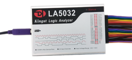
С вероятностью 95% он вам не нужен.
Давно хотел себе купить такой, а началось еще году в 2011 или еще раньше, когда вышел анализатор на мелкасхеме кипариса и китаезы скопировали его. Был такой еще софт usbee. Я даже заказывал набор для самостоятельной сборки. Причем там был еще аналоговый канал с ацп. Недавно смотрел софт на этот анализатор и что-то он совсем старый какой-то. Новые версии выходят под новые анализаторы.
Это новая версия с плисиной и защитой до +-50в и 100 мгц, правда на 2 канала.
Ахтунг. Это не совсем клон китайский. Это как бы собственная разработка китайцев. У них даже свой сайт есть.
www.qdkingst.com/en
Сегодня даже скачалось обновление.
Есть другой клон с похожим софтом и тремя светодиодами и без шим. В этом даже 2 канала шим есть.
У меня пришло 3 комплекта силиконовых проводов по 8 штук. Видать лишнее кинули. Клипс 5 штук. Только штырьки короткие и провода слетают. Провода очень хорошие на ощупь и легко гнутся.
Усб кабель тоже очень хороший. На высоких скоростях плохие кабеля не могут прокачать большой поток, так что вставляйте в компутер напрямую, а не через хаб и обязательно толстый кабель.
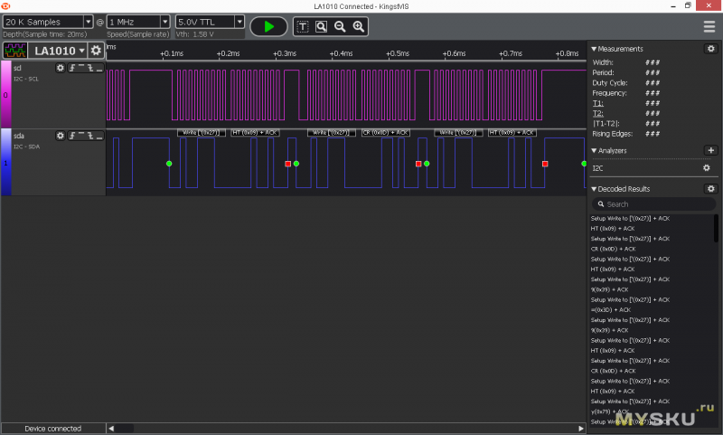
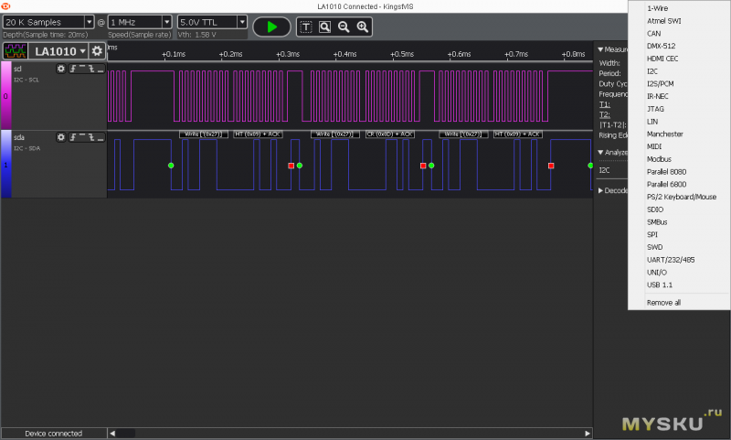
Вот я попробовал и2ц.
Можно разглядеть адрес 0х27. Это адрес платки расширителя портов, которая прилеплена к жк индикатору.
Ну и список протоколов. Можно самому запилить протокол. Есть даже мануал на русском, как это делать.
Скрол и увеличение времени развертки делается колесиком. Эта прога более легкая и не тормозит по сравнению с другой версией анализатора Saleae.
В данном случае зеленая точка показывается условие «старт» на шине и красная точка означает конец передачи пакета. Эта шина допускает передачу нескольких байт за раз, когда передается адрес устройства и эти маркеры тут очень полезны окажутся.
Вобщем анализатор норм, с запасом на будущее лет на 10. Думаю защита убережет его в течении этого времени.
Ну и самый главный минус всех этих анализаторов — отсутствие генератора сигналов или правильней они называются pattern generator. Это когда можно эмулировать протоколы или устройства и такой анализатор превращается в генератор данных для разных шин. Причем без аппаратной переделки, т.к. кипарис этот не совсем обычный контроллер, а в него заливается прошивка в момент подключения и старта проги. Там даже некоторое время проходит и видно окошко с прогрессбаром. Ну и плис тоже вроде как прошивается налету.
Думаю в будущем может допилят софт.
Планирую купить
+19
Добавить в избранное
Обзор понравился
+33
+48
Описание
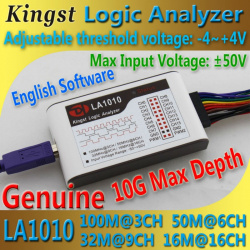
Kingst-LA1010 — это высокопроизводительный логический анализатор, имеющий 16 входных каналов и частоту выборки до 100 МГц. В комплекте идет CD диск с программным обеспечением KingstVIS, для установки на ПК. Анализатор поддерживает множество стандартных протоколов и может применяться для тестирования и анализа цифровых систем (MCU/ARM/FPGA, и др.), разработки и отладки нескольких коммуникационных программ, а также для длительного мониторинга и записи цифровых сигналов.
Особенности:
Портативный и легкий
Максимальная частота дискретизации: 100M @ 3 канала, 50M @ 6 каналов, 32M @ 9 каналов, 16M @ 16 каналов
Большая глубина выборки и сжатие
Встроенный генератор ШИМ
Совместимый интерфейс USB2.0 / 3.0
Мощное и простое в использовании программное обеспечение
Автоматическое обновление (онлайн)
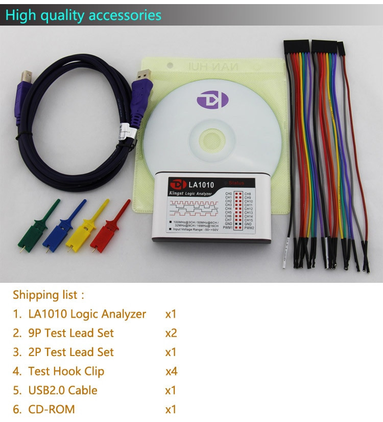
Комплектация
1. LA1010 Host — 1шт.
2. 9P Плоский кабель — 2шт.
3. 2P Плоский кабель — 1шт.
4. Тестовая клипса — 4шт.
5. USB-кабель — 1шт.
6. CD-диск — 1шт.
Product Selection of Logic Analyzer
| Product Model | LA1010 | LA2016 | LA5016 | LA5032 |
| Product Photo | 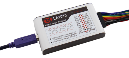 |
 |
 |
 |
| Purchase Link |
$68.00 |
$138.00 |
$238.00 |
$398.00 |
| Channel Number | 16 | 16 | 16 | 32 |
| Max Sampling Rate | 100M@3CH, 50M@6CH 32M@9CH, 16M@16CH |
200M@16CH | 500M@16CH | 500M@32CH |
| Fastest Digital Signal | 20MHz | 40MHz | 80MHz | 80MHz |
| Min Pulse Width | 20ns | 12.5ns | 6.25ns | 6.25ns |
| Hardware Memory Size | — | 1G bits | 2G bits | 4G bits |
| Hardware Sampling Depth (can be ensured) |
— | 50M Sas | 100M Sas | 100M Sas |
| Max Compression Depth (can’t be ensured) |
10G Sas | 10G Sas | 10G Sas | 10G Sas |
| Threshold Voltages | -4V ~ +4V | -4V ~ +4V | -4V ~ +4V | -4V ~ +4V |
 |
|
| Status | supported |
|---|---|
| Source code | kingst-la2016 |
| Channels | 16 — 32 |
| Samplerate | 100MHz — 500MHz |
| Samplerate (state) | — |
| Triggers |
Level (multiple channels) Edge (one channel) |
| Min/max voltage | -50V — 50V tolerant |
| Threshold voltage | -4.0V—+4.0V, min step 0.01V |
| Memory | 0Gib — 4Gib RAM (0-512MiB) |
| Compression | Yes |
| Website | qdkingst.com |
The Kingst LA Series spans across a set of USB based, 16 or 32 channel logic analyzers with 100MHz to 500MHz maximum samplerate and up to 1Gib to 4Gib (128MiB to 512KiB) sample memory, one of the models without any local memory. One common kingst-la2016 sigrok driver supports all devices in the series.
Several devices share the same USB VID:PID identification. It even appears as if these values are not specific to the logic analyzers: Linux’ lsusb command «mistakes» these as a camera (though this is just a matter of display text presentation, neither a functional limitation nor a conflict).
Kingst LA models can either capture to local memory first and upload sample data to the host afterwards (when the model has local memory). Or alternatively can stream samples to the host while the capture is being taken (the USB channel limits the product of samplerate and enabled channels that can get communicated).
Devices
| Device name | samplerate | channels | memory | supported |
|---|---|---|---|---|
| Kingst LA1010 | 100 MHz | 16 ch | — | untested |
| Kingst LA1016 | 100 MHz | 16 ch | 128 MiB | tested |
| Kingst LA2016 | 200 MHz | 16 ch | 128 MiB | tested |
| Kingst LA5016 | 500 MHz | 16 ch | 256 MiB | tested |
| Kingst LA5032 | 500 MHz | 32 ch | 512 MiB | tested |
Most of the support became available in 2022-02, versions before that date may only support individual models. LA5032 support got unbroken in 2022-10.
Hardware
TODO Move the common part of the hardware from Kingst LA2016 here.
Most devices share some fundamental properties. Differences are few.
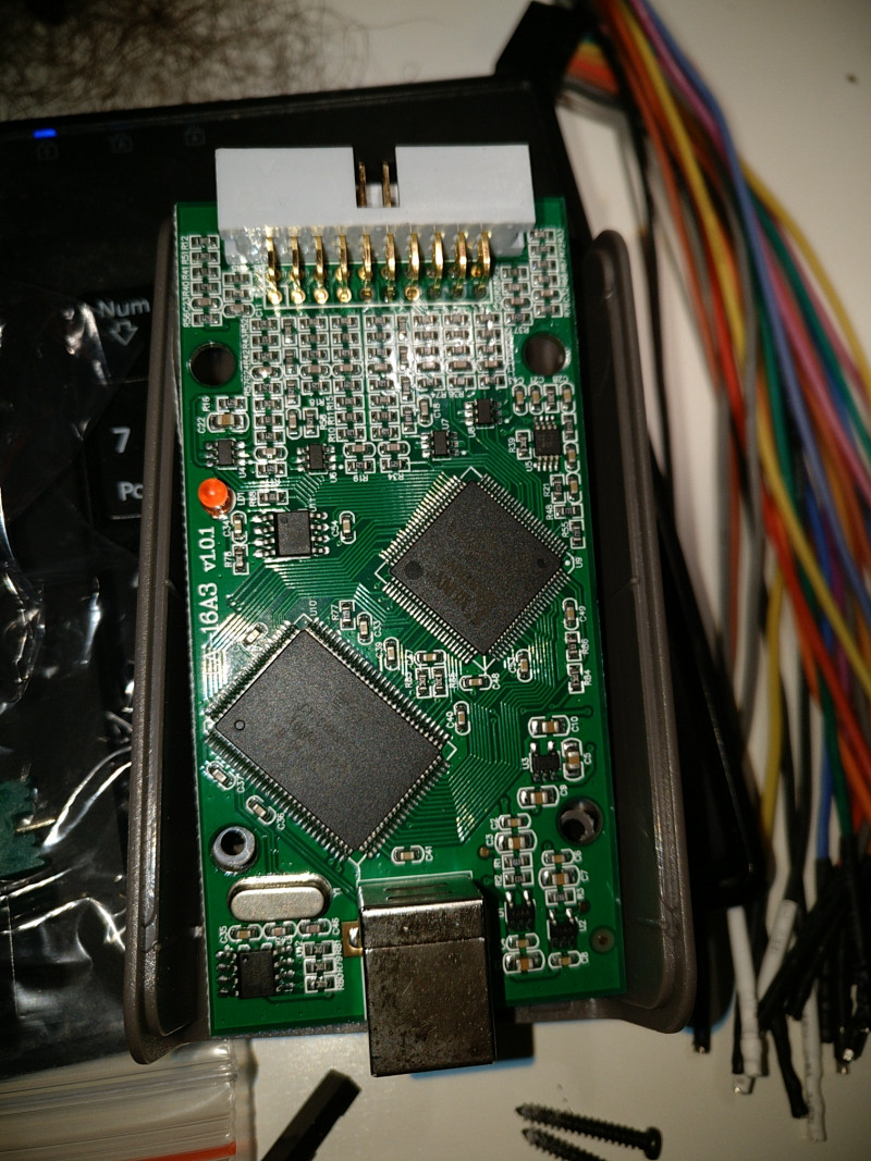
- Cypress FX2 MCU
- Cyclone IV FPGA
- Samsung(?) DRAM
- AT24 EEPROM
- U10 «hardware dongle»
- voltage regulation
- opamp, input threshold control
- TVS diodes
The LA1016 and LA2016 devices are said to have identical hardware, only their FPGA firmware differs. TODO The LA1010 may or may not share the LA1016 hardware, the base clock could be an internal implementation detail of the FPGA. The LA5016 and LA5032 devices may or may not share hardware (input protection for the upper 16 channels and additional memory may reside on the bottom layer). These details need verification when these models are seen in the field.
The internal implementation of clocks differs across models. The LA1010 uses an 800MHz base clock and supports up to 100MHz samplerate. The LA1016 and LA2016 devices use a base clock which is identical to their 100MHz/200MHz maximum samplerate. The LA5016 and LA5032 use an 800MHz base clock to derive their samplerates from, while a divider of 1 will result in a 500MHz samplerate, divider 4 is used for 200MHz samplerate.
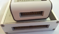
For images which show the cases, connectors, and PCBs see the individual devices’ pages. The models up to 200MHz come in a plastic case with a smaller outline and a 20pin connector for the logic probes and PWM. The 500MHz models have a larger PCB and a 40pin connector in a metal case.
Photos
-

LA2016 mugshot
-

LA5016 mugshot
-

LA5016 and LA2016 side by side
-

LA5016 and LA2016 probe connectors
Protocol
Several devices share the same USB identification (VID and PID). The PID determines which FX2 MCU firmware to upload to the device. Once the MCU firmware is in place (which involves USB renumeration), USB communication can access EEPROM content, which allows to identify the device type. Which determines the device’s capabilities (maximum samplerate, channel count, memory depth), and the FPGA bitstream to upload to the device. The FPGA logic will automatically verify its matching the device hardware by communicating to IC U10, loading non-matching bitstreams will not enable features which the device does not provide in its proper configuration.
The device’s firmware provides two (three) USB endpoints. EP2 is write only and is used to upload FPGA bitstreams. EP6 is read only and downloads captured sample data by means of USB bulk transfers. EP0 supports USB control transfers to configure the device and supervise its operation.
Acquisition is completely driven by the device’s hardware. A configuration gets sent to the device, specifying enabled channels, samplerate, samples count, trigger parameters. The hardware acquires data from the logic probes and writes it to local RAM. After the acquisition has completed, the host can download the captured data. Hardware compression is transparent, some 50MSa are guaranteed (model dependent). Oversampling and slowly changing input data can result in the ability to squeeze a few hundred MSa into RAM before the memory capacity is exhausted, this heavily depends on the input signal’s pattern. The announced 10GSa capacity with compression enabled is a theoretical value that is hardly seen in practice.
All devices in the family support streaming mode. Most of them in addition to or as an alternative to local storage before download, the memory-less LA1010 as the only supported mode of operation. All of the preparation (device identification, firmware download, acquisition setup, sample data upload from USB endpoint 6) is identical to «normal mode» as the vendor calls it. But sample data upload immediately starts when the acquisition gets initiated. The device will neither use local memory for buffering, to compensate for bursts in the input data and slow USB communication to the PC. Nor will the device apply RLE compression on the sample data. Bits only get shifted in ways similar to Saleae-Logic16 to reduce the amount of USB traffic while uncompressed data gets communicated (disabled channels need not get sent, but enabled channels’ data is not compressed). Successful reception of sample data in streaming mode heavily depends on the whole chain from the device to the host application and its capability to process the steady USB communication at high Mbps rates. The vendor software assumes a limit of some 300Mbps (sample rate multiplied by the number of enabled channels).
Many of the FPGA registers are read-only or write only, which prevents reading back a configuration that previously was written to the device. When registers support read and write, their meaning differs depending on the direction of data exchange. This means that sigrok software cannot re-use a previous configuration across sessions, instead always needs to start from default values. This is a limitation of the vendor firmware, not the sigrok driver.
See Kingst LA2016/Protocol for more developer notes and captures that were taken during protocol research.
Firmware
In order to use this device you need to extract the firmware/FPGA files from the vendor software (Linux download) using the sigrok-fwextract-kingst-la2016 script from the sigrok-util repo and place them in one of the usual places where libsigrok expects firmware files:
$ ./sigrok-fwextract-kingst-la2016 KingstVIS/KingstVIS
saved 5430 bytes to kingst-la-01a2.fw (crc32=720551a9)
saved 178362 bytes to kingst-la2016a1-fpga.bitstream (crc32=7cc894fa)
saved 178542 bytes to kingst-la2016-fpga.bitstream (crc32=20694ff1)
...
Resources
- Vendor software
- User guide
- Reverse engineered schematic
It is essential to use logic analyzers for embedded drive development.
What happens to use a logic analyzer
When you write a driver and device communication read and write data, you can use a logical analyzer to exclude hardware problems so that we can follow the software’s bug.
Here I use Kingst Logic Analyzer LA1010 Model as an example to explain.
Connection hardware
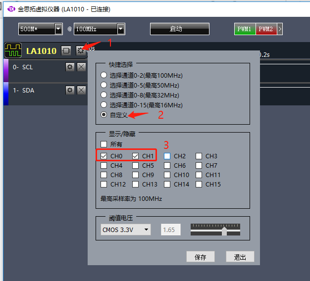
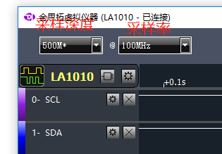
The logic analyzer is compared to the wave, the volume is obvious, first of all, you need the hardware engineer to help you lead the board from the three line SCL (clock line) SDA (data cable) GND (ground).
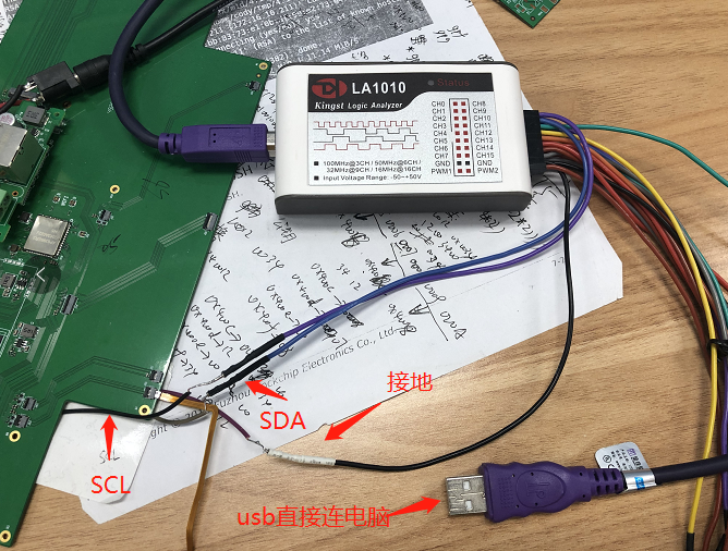
The logic analyzer USB is directly connected to the computer, then selects two CH channels to connect to SCL and SDA. Here I will connect the CH0 even SCL, CH1, and the ground line corresponds to the GND of the logic analyzer.
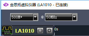
Logic analyzer software settings
Provides this software by logic analyzer manufacturers
As shown in the figure, the software is working properly.
Set the channel we use, save exit
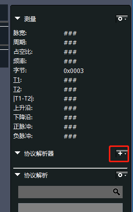
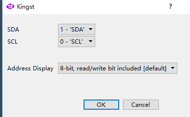
Add a protocol parser, select I2C
SDA and SCL choose correct
Set the sampling rate and sampling depth, there are two ways to improve the collection time, one is to increase the sampling depth, the second is to reduce the sampling rate
Send commands using I2C Tool Tools
Direct ADB PUSH to the board
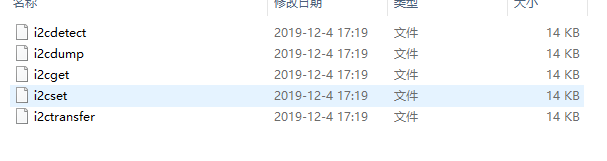
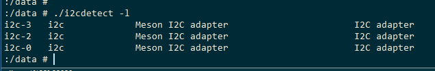
Several groups of I2C on the detection system
Command: i2cdtect -l can see the current board, three groups of I2C is available
Detects the device mounted on the I2C
Command: i2cdetect -r -y 0 Detects the device on I2C0
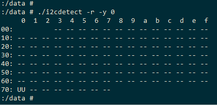
You can see that there is a device on the address of 0x70, which is the temperature and humidity sensor I added.
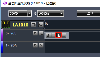
Read 16-bit register (focus) using I2CTransfer
Before performing this step, let’s set the SCL as the falling edge, then start, the software will wait to trigger
Adb shell execution ./i2ctransfer -f -y 0 W2 @ 0x70 0x78 0x66 trigger (where parameter 0 is I2C0, W2 means writing two bytes, @ 0x70 is your I2C device (note to 7th address), 0x78 0x66 is Read the address of the temperature and humidity sensor data)
If the collection time is too short, refer to the appeal method, improve the collection time

If the hardware communication is normal, we put the mouse in the waveform area, hold down the CTRL button slide the mouse pulley, and can zoom in and reduce the waveform. We continue to shrink the waveform, you will find the following graphics, the previous paragraph sends 0x7866 commands for me, and then the data returned by the temperature and humidity sensor.

It can be seen after the waveform is enlarged.
First paragraph

Second paragraph

In the right protocol parses, you can clearly see the data of WiRTE READ.

Can collect such data, the hardware is OK. If we write the driver does not get the data, you should check if our code is problematic.